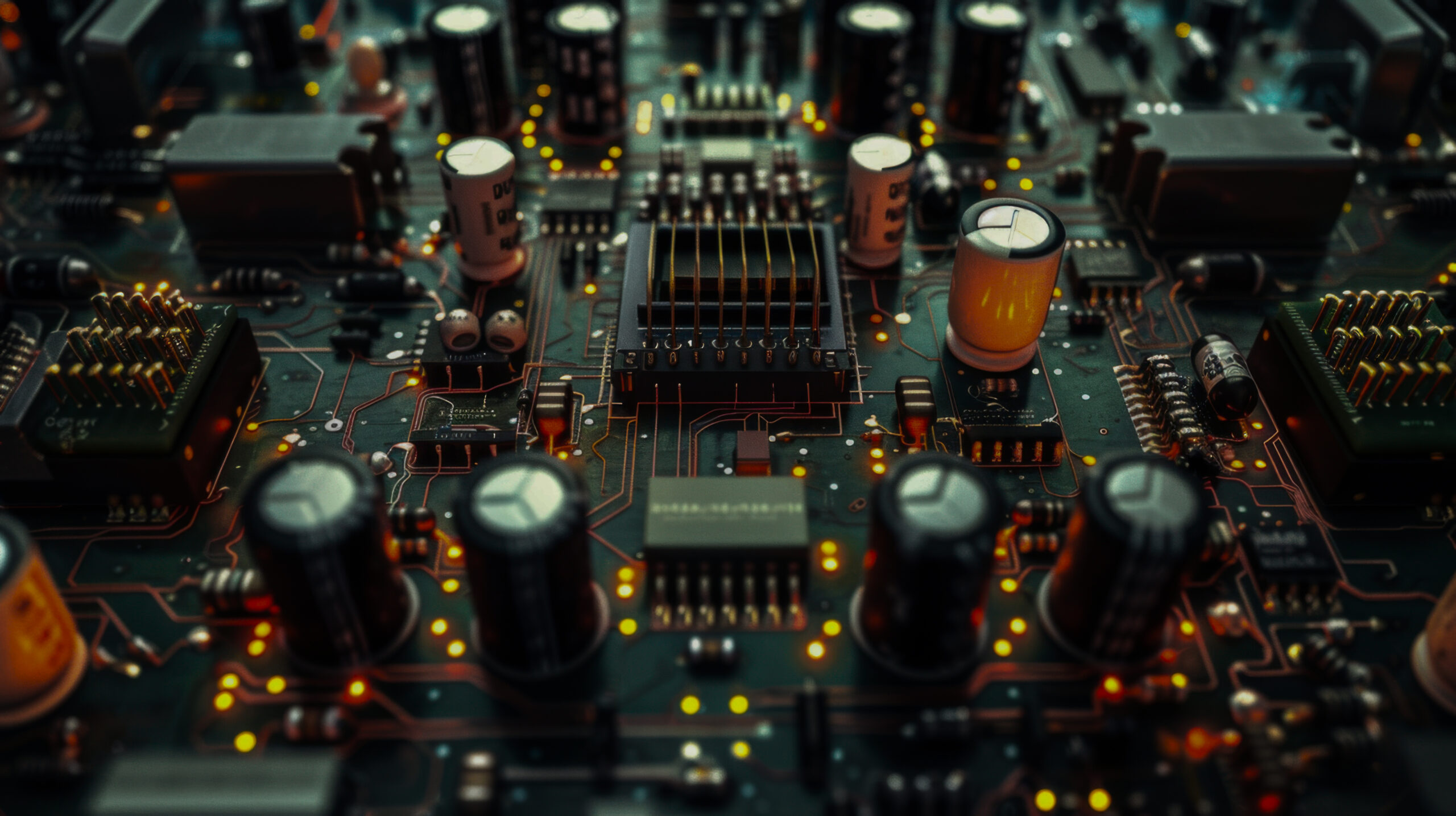
As electronics continue to shrink while performance expectations skyrocket, heat has quietly become one of the biggest design challenges. From AI servers to compact IoT devices, high-density systems pack more power into smaller footprints, inevitably leading to thermal stress.
If not managed properly, heat doesn’t just reduce efficiency; it shortens component lifespan, degrades signal integrity, and can even cause catastrophic failure. In fact, even a 10°C rise in temperature can significantly reduce the lifespan of electronic components.
Let’s explore how modern engineering is tackling this challenge with advanced heat dissipation strategies.
Why Heat Management Matters More Than Ever
High-density PCBs (Printed Circuit Boards) are designed to integrate more components into tighter spaces. While this boosts performance and miniaturization, it also creates concentrated heat zones with limited airflow.
This is where smart PCB engineering comes into play. Engineers today must think beyond electrical performance and treat thermal management as a core design parameter, not an afterthought.
Thermal Management Strategies for High-Performance PCBs
Smart Layout: The First Line of Defense
Before adding any cooling hardware, effective thermal control begins at the design stage.
Strategic component placement ensures heat-generating elements like processors and power modules are not clustered together. Spreading them across the board reduces hotspots and allows heat to dissipate more evenly.
Layer stack optimization also plays a key role. Using internal copper planes as heat spreaders helps distribute thermal energy across the board, lowering localized temperature buildup.
A reliable PCB design service will always integrate thermal simulation early in the design phase to predict and eliminate potential heat issues before manufacturing.
Thermal Vias: Small Features, Big Impact
Thermal vias are one of the most effective and widely used techniques for heat dissipation in dense PCBs.
These tiny, copper-filled holes transfer heat from hot components to other layers or heat sinks. When placed correctly, especially under high-power components, they create a direct pathway for heat escape. Studies show that thermal vias can reduce junction temperatures by up to 10–25°C, depending on density and design.
In advanced custom PCB design, via arrays are carefully optimized to balance thermal performance with structural integrity.
Advanced Materials for Better Heat Flow
Material selection can make or break thermal performance.
Traditional FR-4 substrates offer limited thermal conductivity (~0.3 W/m·K), which is often insufficient for high-power applications.
Modern solutions include:
- Metal-core PCBs (aluminum or copper cores)
- Ceramic substrates with higher conductivity
- High-Tg laminates for improved thermal resistance
These materials significantly enhance heat transfer, making them essential in high-performance PCB engineering applications.
Heat Sinks, Spreaders, and Interface Materials
When passive board-level techniques aren’t enough, external cooling solutions come into play. Heat sinks increase surface area, allowing heat to dissipate into the surrounding air. Copper heat sinks, for example, can reduce component temperatures by up to 25°C.
Thermal Interface Materials (TIMs), such as pads or pastes, improve contact between components and heat sinks, reducing thermal resistance and enhancing efficiency.
In a well-executed PCB design service, these elements are not just added; they’re precisely matched to the system’s thermal profile.
Active Cooling for High-Power Systems
As power densities increase, passive cooling alone often isn’t enough.
Active cooling solutions include:
- Miniature fans for forced airflow
- Liquid cooling systems for extreme heat loads
- Thermoelectric coolers for precise temperature control
Even small fans can reduce temperatures by 10–30°C in confined systems.
These solutions are commonly used in data centers, automotive electronics, and telecom infrastructure, where reliability is critical.
Cutting-Edge Innovations in Thermal Management
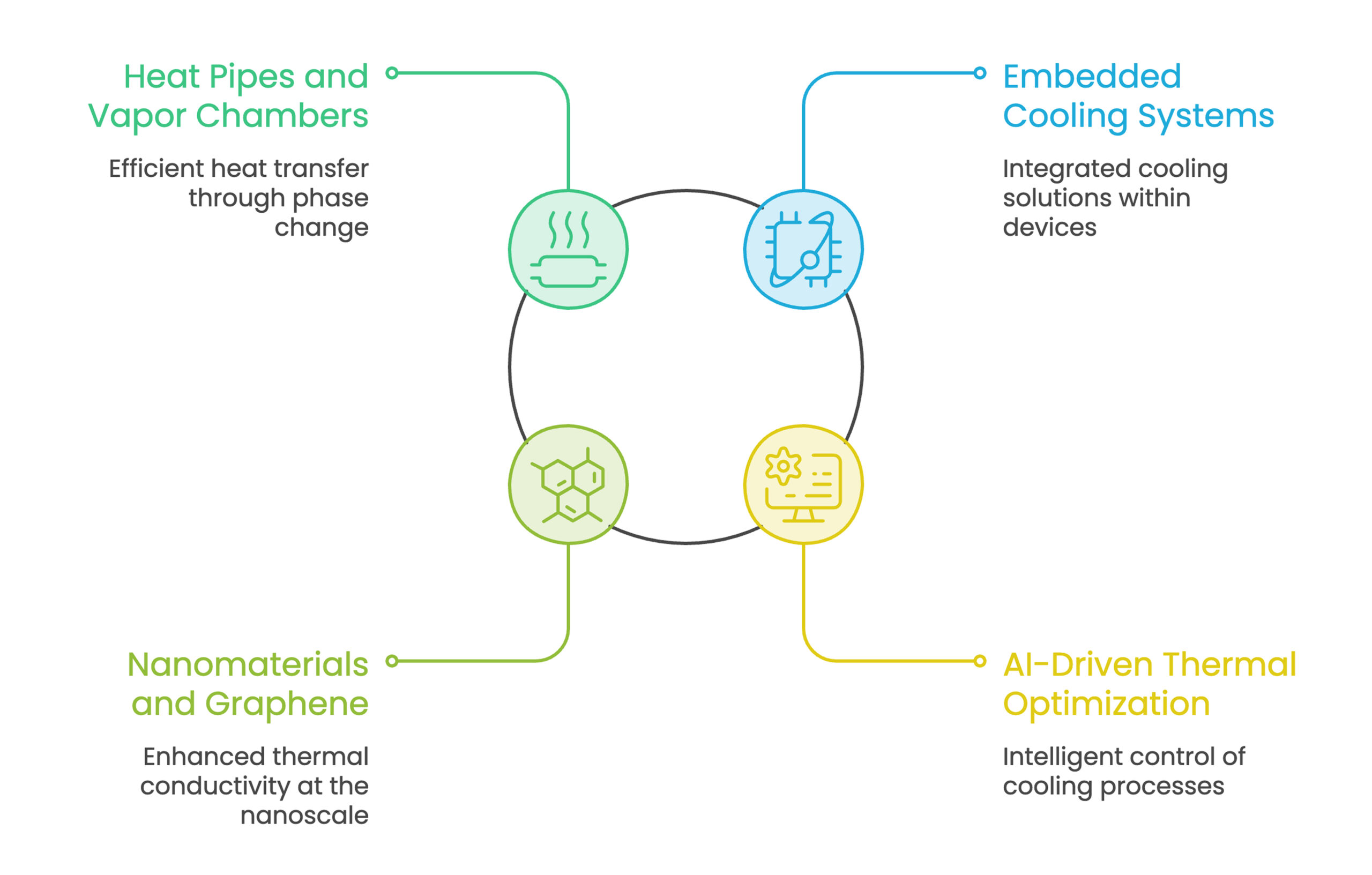
The future of thermal management is being shaped by breakthrough technologies:
1. Heat Pipes and Vapor Chambers
These use phase-change cooling to transfer heat extremely efficiently, outperforming traditional methods by a wide margin.
2. Embedded Cooling Systems
Microchannels and embedded liquid cooling within PCBs allow direct heat removal, reducing temperatures by up to 30°C.
3. Nanomaterials and Graphene
Advanced materials like graphene offer exceptional thermal conductivity, enabling faster heat spreading across compact designs.
4. AI-Driven Thermal Optimization
AI systems can dynamically adjust cooling mechanisms based on real-time thermal data, improving efficiency and reducing energy consumption.
These innovations are redefining what’s possible in custom PCB design, especially for next-generation electronics.
The Role of Simulation and Testing
No thermal strategy is complete without validation.
Modern tools allow engineers to simulate airflow, heat distribution, and thermal resistance before physical prototypes are built. This reduces design iterations, saves cost, and ensures reliability.
Thermal testing, both at component and system levels, helps verify real-world performance under different operating conditions.
This is where a professional PCB design service proves invaluable, combining simulation expertise with real-world testing capabilities.
Balancing Performance, Cost, and Reliability
Thermal management is always a balancing act. High-end solutions like liquid cooling or advanced materials offer superior performance, but at increased cost and complexity. On the other hand, optimized layouts and thermal vias provide cost-effective improvements.
The key lies in choosing the right combination based on:
- Power density
- Form factor constraints
- Environmental conditions
- Budget considerations
This is why experienced PCB engineering teams focus on holistic design rather than isolated fixes.
How Tessolve Powers Advanced Thermal Solutions
At Tessolve, we understand that thermal management is not just a design requirement; it’s a performance enabler.
Our end-to-end PCB design service integrates advanced thermal analysis, simulation, and optimization right from the initial concept stage. With deep expertise in PCB engineering, we design high-density systems that balance power, reliability, and heat dissipation seamlessly.
From material selection to thermal via optimization and advanced cooling integration, our approach to custom PCB design ensures your products perform reliably even under extreme conditions.
Whether you’re building next-generation automotive systems, AI hardware, or high-speed communication devices, Tessolve delivers thermally optimized designs that stand the test of real-world demands.
Frequently Asked Questions (FAQs)
1. Why is heat dissipation important in high-density PCBs?
Effective heat dissipation prevents overheating, improves performance stability, and extends the lifespan of sensitive electronic components.
2. What are thermal vias, and how do they help?
Thermal vias are small conductive holes that transfer heat away from components, reducing hotspots and improving overall thermal performance.
3. Which materials are best for better heat management in PCBs?
Materials like metal-core substrates, ceramics, and high-Tg laminates offer better thermal conductivity than standard FR-4 boards.
4. When should I consider active cooling solutions?
Active cooling is useful when passive methods aren’t enough, especially in high-power, compact, or continuously operating electronic systems.
5. How can a PCB design service improve thermal performance?
A professional PCB design service uses simulations, optimized layouts, and material selection to manage heat efficiently from early design stages.