Fortifying chip’s integrity with state-of-the-art tech
Facility Overview
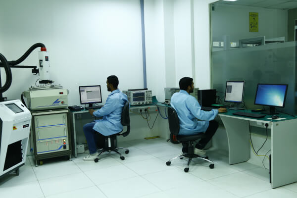
Robust infrastructure and precise verification ecosystem
Tessolve is a one-stop place for Semiconductor companies to perform Testing, Debugging, and Characterizing the devices using advanced technologies in a cost-effective, Speedy way. Our semiconductor lab facilities provide some of the unique value added services, offered only by a few in the region.
Diverse Facilities
Made available and accessible under one roof
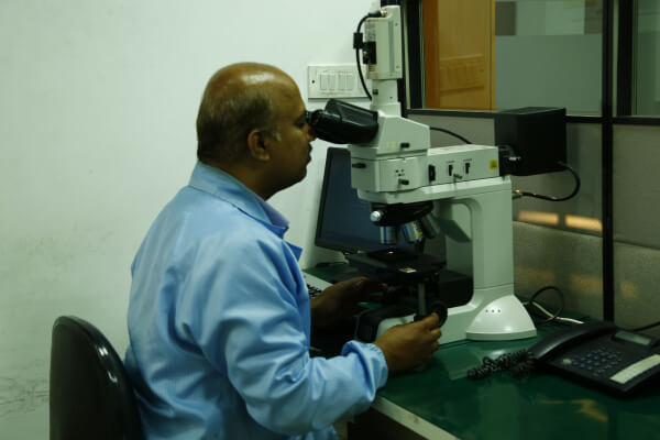
Optical Microscopy – an expensive equipment to analyze chip layout, Bonding arrangement, etc.
Characterization Lab is a unique facility in India to perform complete Electrical Level characterization of Silicon Devices and is aided by the Government Of India.
Best Practices
Enablers of global-standard quality assessment
Our state-of-the-art equipment, analytics services and our value added activities allow us to perform reliability assessments and provide you with actionable insights.
Facilities At A Glance
Showcasing state-of-the-art-tech we’re proud of
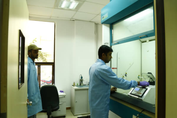
Failure Analysis
Exposing semiconductors for analysis is challenging. Qualified de-capsulation processes and certified tools are mandatory. We have experienced engineers specialized in analyzing the failure and Providing the root cause to the customer. We have developed chemical recipes for all the package families. Cu protect de-capsulator equipment (Nisene) is a patented machine targeted for the latest and most complex package.
- De-capsulation of all Plastic Package
- 1000X Optical Microscopy for Full HD image
- Polyamide Removal
- Selective area de-capsulation
- Measuring software for measuring package/die dimension
- Package Cross sectioning for analysis
- Epoxy filling after FIB edit and UV eraser
- Die/PCB cross-section analysis
- 3D X-Ray imaging
- BGA Rework
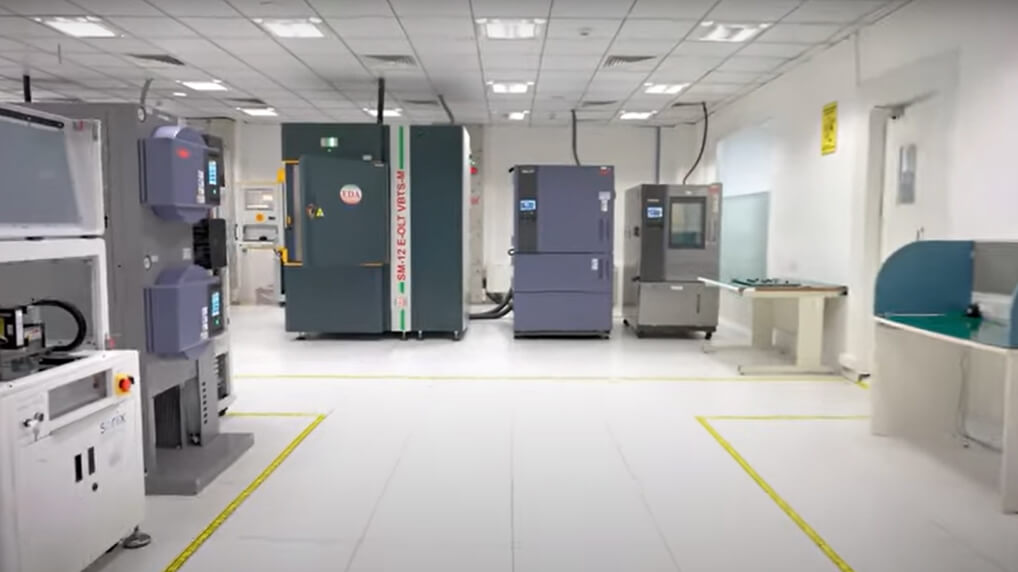
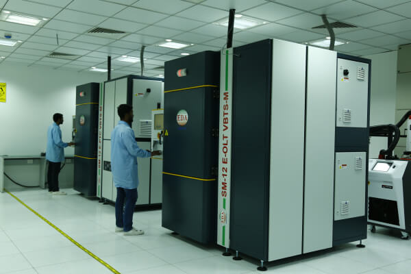
Semiconductor Environmental Stress Testing Tool
One stop solution for Product/Package Qualification
- HTOL (High Temp Operating Life Test)
- LTOL (Low Temp Operating Life Test)
- ELFR (Early Life Failure Rate)
- HTSL (High Temp Storage Test)
- ESD Simulation (HBM, MM & Latch-up)
- Bake Oven (Moisture Remove)
- TC (Temperature Cycling)
- HAST ( bHast / uHast )
- TCT (Thermal Shock)
- THB (Temperature Humidity Bias)
- PTC (Power Temp Cycling)
- We have partnered with 3rd part lab for CSAM & Reflow
- Standards: JEDEC, IEC, AEC
Package Expertise
Varied test packages our experts excel at


Equipments We Leverage
Latest devices – best for verification
Decapsulation
- Selective Area Decapping
- Polyamide Removal
- Bond Wire Integrity After Decapsulation
- Selective Area Decapping
Optical Microscopy
- Magnification Up To 1000x
- Bright/Dark Field
- Measurement Software
Other Analytical Services
- Failure Verification
- Fault Localization
- Sample Preparation and Defect Tracing
- Defect Characterization


