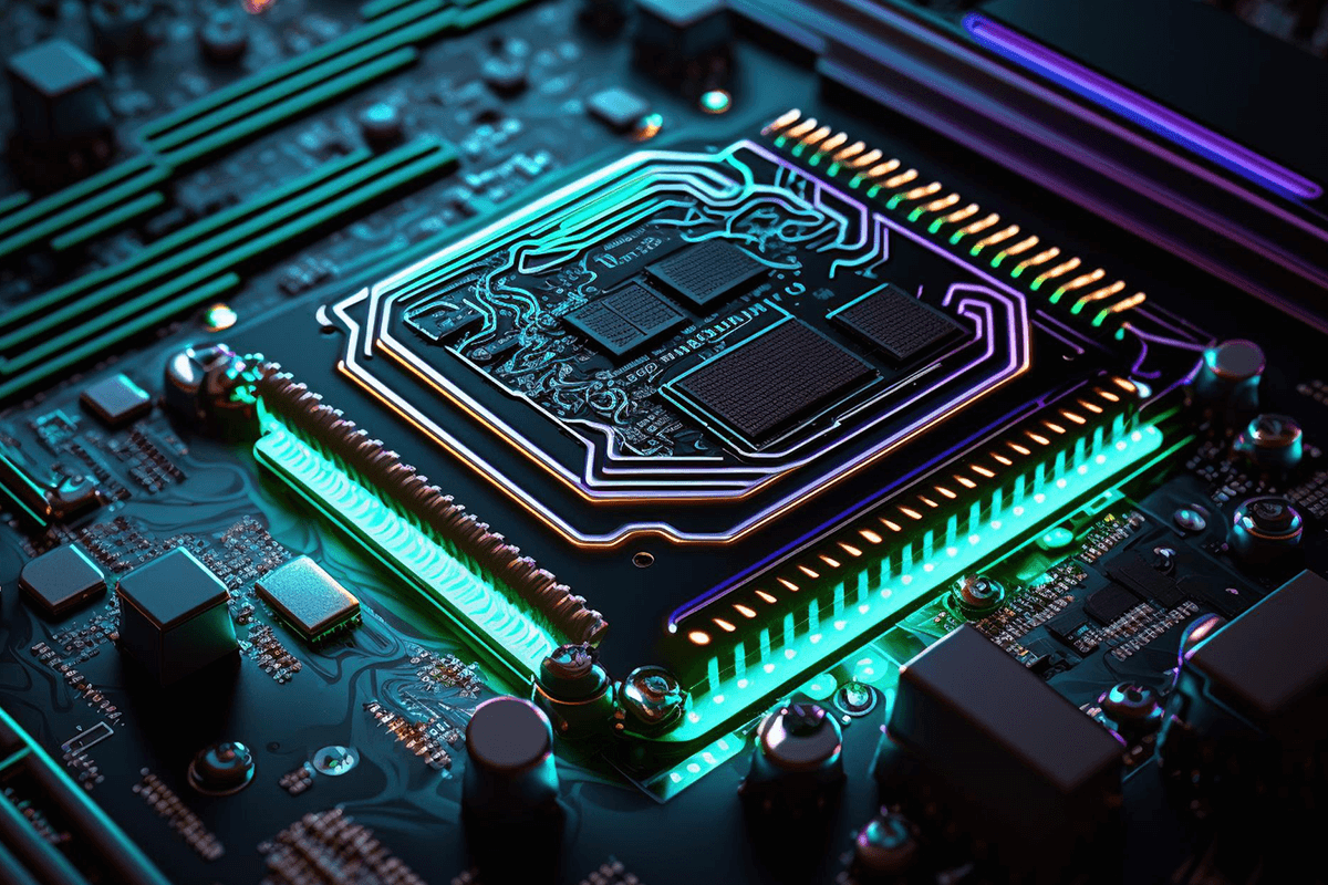
Igniting the next wave of semiconductor performance
HSIO Lab Overview
Pioneering high-speed I/O solutions for transformative semiconductor advancements
To advance industry trends for Consumer, Automotive, Gaming, and Enterprise Markets, Tessolve partners with Keysight to provide HIGH-SPEED I/O interconnect test solutions. This collaboration will enable customers to drive semiconductor innovation, through improved testing capabilities at Tessolve’s newly established HSIO Lab. Through the HSIO Lab’s expertise, semiconductor companies can unlock significant performance gains, pushing the boundaries of what is possible.
Key drivers for the establishment of the HSIO lab:
- Pushing Video Quality beyond 8K
- Gaming an VR requirements for low latency
- Internet of Things” (IoT) drives the enterprise market for streaming and cloud applications requiring High data rates for server/storage-related solutions.
Developing cutting-edge test solutions @112Gbps data rate requires close collaboration and involvement with experienced high-speed IO experts. Working together with our mutual customers, Tessolve and Keysight can leverage the strengths of both companies to help ensure success and provide the full benefits by leveraging the SI Analysis & mmWave board design expertise.
Facility Overview
Fueling technological advancement through next-gen HSIO testing
To elevate the journey and the strength to the next level, Tessolve invested in 70GHz
Test instrumentation with keysight technologies to provide cutting-edge test solutions to their customers on
HSIO domain LPDDR/DDR5, USB 4.0, PCIe Gen 6, etc. It helps to perform a wide variety of signal integrity parameter
measurements apart from SERDES Tx & Rx Compliance measurements. Name the few here, –

Jitter and measurement analysis

Embedding and De-embedding
S-parameters

Equalization and crosstalk analysis

Real-time eye diagram and advanced
clock recovery

Transformation of time domain signals into
a frequency domain

Analysis of NRZ and PAM-N signals

CEM tests

Link EQ tests

PLL Loop bandwidth and peaking tests
HSIO test involves measurement of Tx eye characterization, receiver tests using BERT and interference signals checking ability to detect a low-level signal, and confirmation that continuous time linear equalization (CTLE) and other equalizations and thresholds are effectively compensating for insertion loss. In addition, the error detector must verify the bit error rate and confirm that a receiver can receive an off-frequency or out-of-phase signal.
Key Benefits
Empowering semiconductor industries to achieve unprecedented performance

The HSIO lab which is the result of collaboration between Tessolve and Keysight brings a few key benefits to industry, customer base, and business to both under a win-win strategy.
- Standard and Complex IP Block Design and Development
- SoC and Sub-system Integration, Clock and Reset design, Clock gating, Low-power design, UPF definition
- RTL Quality Checks: Lint, CDC, Automated property checks, Low-power checks
- Protocol Experience: HSIO Protocols (PCIe, USB, MIPI), AMBA protocols (AXI/AHB/APB), Memory interfaces (DDRx/LPDDRx), Low-speed peripheral interfaces (I2C, SPI, UART, MDIO, I2S)
Tessolve Strength
Your Gateway to Next-Gen Semiconductor Performance

Tessolve has 22+ years of experience in the semiconductor global space; we have a strong footprint in chip design, and pre- & post-silicon validation. HSIO is an integral part of the SoC, and Tessolve has strong expertise in this domain.

Tessolve empowers various OEMs with Chip Design, ASIC design, and pre-silicon and post-silicon validation.

Tessolve is on the journey of providing cutting-edge test solutions to its customers on various HSIO technologies such as PCIe Gen6, DDR5 SDRAM, USB 4.0, etc.
Simulating multiple signal frequencies and data rates when combined within a common application has many challenges with signal integrity and channel simulators. Tessolve has experience in identifying analytical gaps, and implementing simulation software for targeted RF Frequencies, taking care of EMI, and demonstrated successful solutions across multiple IBIS/AMI models.

While Industries are shifting to a 3nm process to lower the cost and power consumption of chips and computing systems, HSIO Interconnects are crucial as clouds and other computing systems are multiplied and have higher complexity and capability.

Tessolve has advanced SerDes and parallel interface testing methodologies which play a significant role in providing a platform to develop a chip. It helps to improve higher bandwidth, lower latency, Lower bit error rate, and energy efficiency for meeting the demands of Machine learning, AI, and complex emerging gaming virtual worlds.
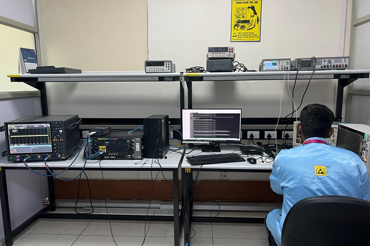
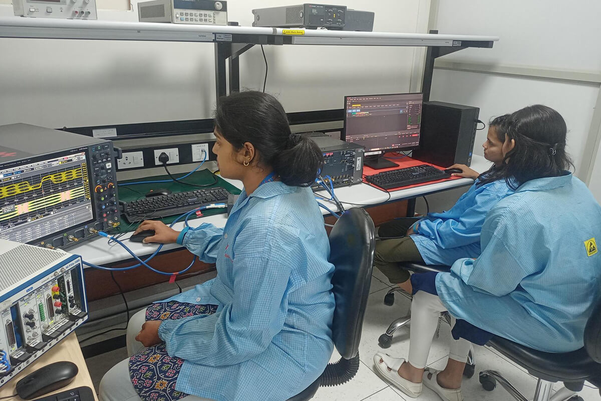
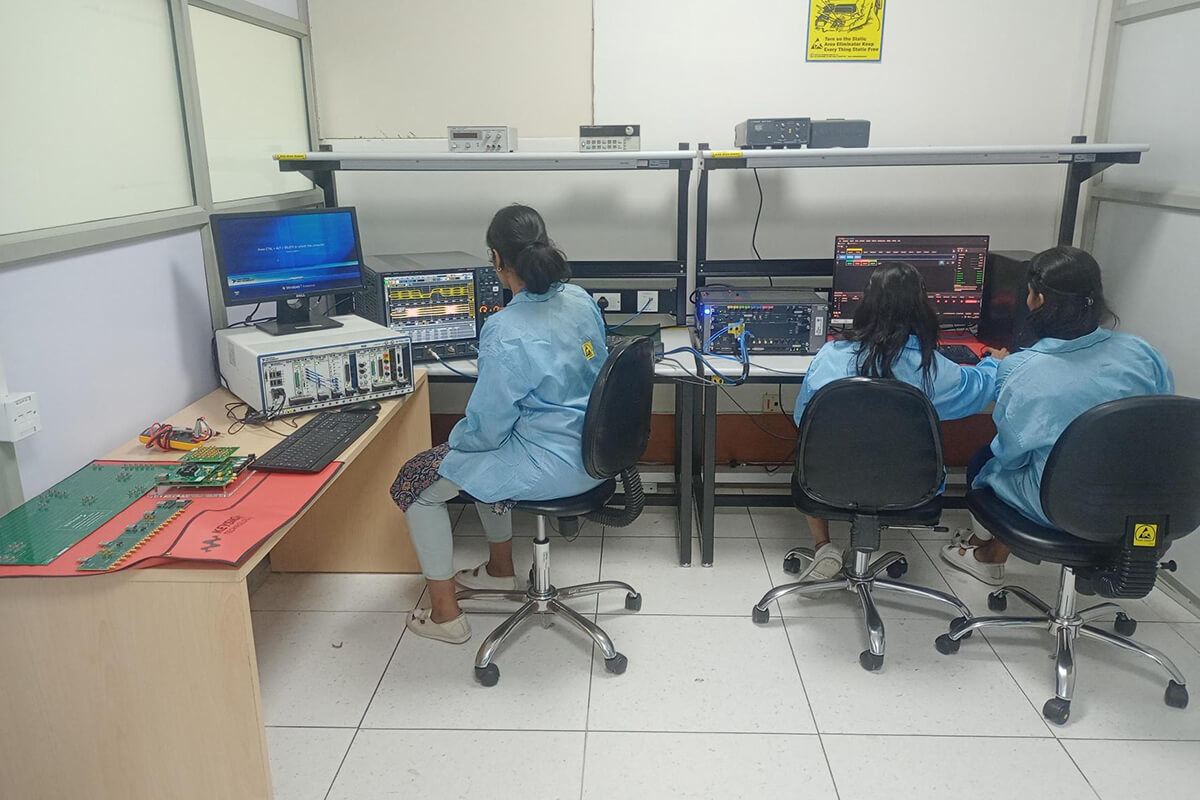
High-Speed Testing Gallery
A gallery of innovation in high-speed interconnect