Advanced packaging solutions for diverse chipsets
Our Calibre In Package Engineering
Designing high-quality IC package solutions
IC Package design is an integral part of chip and package developments. We have designed some of the most advanced, high-performance packages on the market for our industry-leading customers. Tessolve has done package designs for a wide variety of packaging solutions, including:
- Flip Chip Designs
- System in Package (SIP)
- Wire Bond Designs
- 2.5D Package Designs
- Chiplet Design
Outlining Our Competence
Spotlight on perfecting packaging design practice

Addressing customer requirements with design experts developing ultra-high-performance package designs that offer high reliability.

Ensuring bump optimization for better routing optimized BGA pin net assignment, and critical routings ‘meet SI, PI, Thermal and manufacturing requirements, as per the design for manufacturing (DFM) rules.

Diverse experience in a design that includes Analog/digital mix, high-speed digital signals, high power, and radio frequency (RF) Interfaces.
Engineering It Different
We have handled everything, from the simplest to the most complex of package designs, and have ensured the best performance design is delivered to the customer.
Familiarity of delivering diverse package specifics
- LPDDR5
- ADC/DAC
- HDMI
- PCIE Gen5
- High Band-width Memory (HBM)
Competent Toolkits:
- Cadence APD
- Expedition 2.8 version
Scope Of Design Service
Package categories we’re proficient In


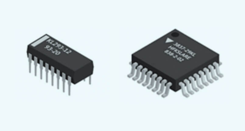
Mechanical Leadframe
Substrate-Based Organic & Ceramic
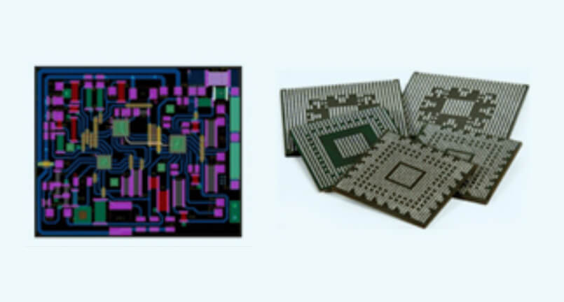
2.5D-IC/Silicon Interposer, Embedded Bridges & FOWLP
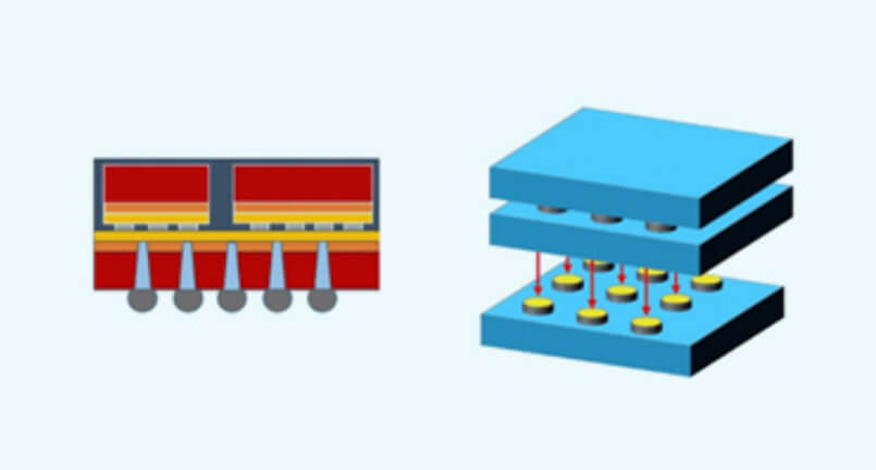
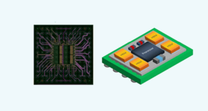
3D-IC
Projects We’ve Delivered
Flipchip BGA design solution
- Up to 18 layers of organic substrate Package size up to 75mmx75mm
- Different types of pitch 0.4mm,0.5mm,0.65mm,0.8mm, and 1mm pitch
- Different types of Heat spreaders that can handle the maximum power dissipation
- Support for High power designs.
- MIPI, CSI, DSI, DDRx, HDMI, PCIEx, ADC, DAC, Serdes interfaces
- High-density complex routing with tight length matching requirement
Our Approach
Proven workflow – with collaborative consulting
Custom consultation and competent support infrastructure help at every stage of the design process – right from die creation to design finalization, validation, and packaging.


