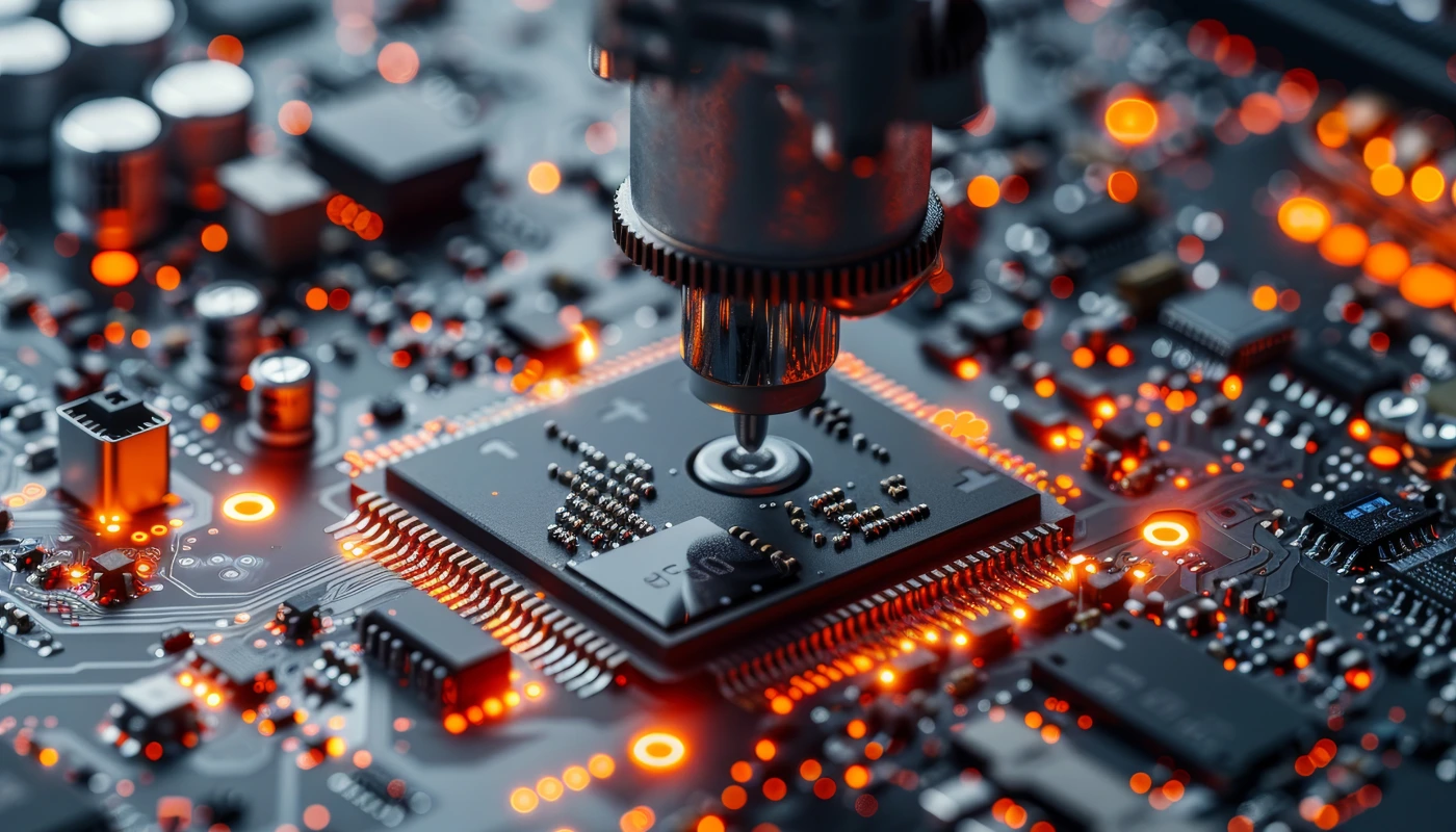
Turnkey PCBs – from Schematic Design to Assembled Boards
Why Tessolve?
Factors that fortify hardware design and delivery
- Tessolve designers are all degreed EE’s who have gone through extensive training before they are allowed to work directly with a customer. It enables them to design PCBs with robust functionality and reliability, and offer top-notch PCB design service and PCB hardware engineering service.
- Tessolve is the leader in High Aspect Ratio PCB board design for Semiconductor, Datacom/Telecom, and Automotive companies worldwide, enabling complex, high-speed, and high-density hardware platforms.
- Tessolve provides high-end production and assembly services through partner and client-qualified Fabs, EMS, and CM companies, delivering end-to-end PCB design service outcomes from concept to production.
- Tessolve is partnered with major EDA companies and offers a complete suite of tools to support any customer with top-notch hardware design.
- Tessolve offers award-winning support and customer service to its clients. This is further strengthened by 24×7 global design support, enabling round-the-clock execution for time-critical and multi-geo programs.
A to Z of PCB Capability
Re-imagined with advances in Technology
- Test Board Design
- System Board Design
- Component Library Services
- Simulation Services
- Mechanical Engineering
Semiconductor Test Board Design
- Swift Design of Cost-effective PCBs for Semiconductor Testing
- Specialist in ATE PCB design board with over 15 years of experience in Test development
- Preferred supplier of the world’s leading Semiconductor companies
- In-house Simulation and Mechanical Engineering team
- Integrated Quality system that has kept our re-designs to <1%
- Clocking in an average of 130 PCB board designs per month
ATE Test Board – Our Design Services
- Load boards (LB), Handler Interface Board (HIB), DUT Interface Board (DIB)
- Probe cards (Vertical / Cantilever), Spider cards, Probe Interface Board (PIB), Flexible PCB boards.
- Device Characterization Boards
- Burn in Boards, HAST, ESD, Latch-up Boards
Board Design Experience
- RF, Analog, High-Speed Digital, Mixed Signal, and Power Management devices
- High Voltage and High Current devices
- HDI Stackup
- Experience in handling PCB materials like Nelco Meteorwave, Rogers, and Megtron series
- Using inventive measures to deliver custom PCB board design
System Board Design
- As a leading hardware PCB board & design company, we develop systems and evaluation boards to help customers evaluate their product functionality before manufacturing.
- Provide application board development using our team’s expertise in High-Speed Processors, Analog, Mixed-Signal, and RF domains.
- Deliver FPGA Emulation and Logic development/porting. Tessolve goes as far as preparing products for certification, ROHS/EMI-EMC.
- We have developed an in-house MAGIK-2 Platform Evaluation Kit.
From custom SOM to product specifications to architecture design, printed circuit board layout, schematics, and assembly planning, our designers take care of it all. We ensure that all our gadgets will be up to your expectations and meet quality standards with reliable PCB design service practices.
Our value-added Services
- Designing hardware for HSIO, 5G, mmWave, PAM4, Si Photonics, High power, 100+ GB/s Data, and Hi-Rel, across a wide range of materials, densities, and component counts.
- We work with Semiconductor, Defense, Automotive, Medical Device, Data/Telecom, IoT, and Consumer product companies.
Boards Supported
RF Applications | Motherboards | Backplanes | Sensor boards | High-Reliability | Evaluation modules | Bench boards | Sub-system boards | Daughter Cards | NPI boards | Avionics Boards
Component Library Services
- A documented footprint of your product design with information on components and detailed specs becomes necessary for design release and modifications.
- Supported by a dedicated library team who are experts in creating a component library from the manufacturer’s datasheet as requested, leveraging a huge collection of Schematic symbols and PCB footprints.
Our Library Services
- Component Library Development, Administration, and Verification
- Library Migration – Legacy to Latest designs with add-on services such as BOM cleaning, Component Obsolescence identification, finding alternates, etc.
Benefits & Highlights
- Footprints developed in strict adherence to IPC-7351 standards
- An innovative parts review process ensures zero defect symbols and footprints
- Dedicated Library development and management team ensure quick turnaround service
- Library documentation conforms to the engineering rules established within IPC-7351
- Automation scripts deployed to ensure quality and reduce cycle time
- In-house developed Library QMS for process standardization
Simulation Services
- We specialize in reading electrical signals to assess the integrity and quality of your PCB design.
- Post-layout analysis is just one option. Our hardware design engineers evaluate alternative layouts even at the pre-design stage.
- Simulation setups and models support this with swift evaluation and defined rules so that the design works under real-world conditions.
- Real-time solving of performance issues and determining the practical level of simulations to eliminate risks and layout iterations – it’s the practice that saves time and cost.
Our Simulation Services
- High-speed Channel Simulations
- Time-domain Waveform Simulations
- Power Integrity Simulations
- Thermal Simulations
- Crosstalk Simulations
- EMI – Radiated Emissions Simulations
- Parasitic RLC Simulations
Simulation Tools Expertise
- Cadence Allegro PCB SI
- Mentor Graphics HyperLynx SI GHz
- ADS SI Pro and PI Pro
Mechanical Engineering
- We cater to multiple market segments with mechanical and electro-mechanical engineering services, and as a result, our capabilities have expanded over the years.
- Our mechanical team can design test fixtures, customized test cells, and develop products. Not to mention the easy validation of design modifications before building any physical prototypes.
- We are ready to take on your electro-mechanical design challenge. Will you accept the Tessolve challenge?
Our Mechanical Engineering Services
- Enclosure Design
- Product/System Architecture
- Shock/Vibration Simulation
- Thermal Simulation and Analysis
- Material and Comp. Selection
- Reverse Engineering with CMM technology, Laser scanning
- Product Specifications drafting
- 3D Rendering and Prototype Design
Printed Circuit Boards
Outlining the team’s turnkey PCB expertise

PCB design company with solutions from schematic design to layout to tested assembled boards with 250+ design engineers globally backed by multi-discipline engineering support.

Complete hardware solutions that encompass in-house QMS (Quality Management System) Tools, Library management systems, Simulation services, and full-turnkey manufacturing.

Our PCB design team consists of systems/hardware engineers across multiple disciplines and time zones, accelerating design cycles with round-the-clock support.

Diverse value-added services – including designing hardware for HSIO, 5G, mmWave, PAM4, High power, 100+ GB/s Data, and Hi-Rel, across a wide range of materials, densities, and components counts.

We increase first pass hardware with an in-house QA and CAM team. Our simulations team offers SI, PI, and Thermal Analysis for complex designs.
Hardware Turnkey Flow
Schematics to the assembling – areas of expertise


Know more about Tessolve's PCB
Design & Manufacturing
Our Expertise
Significant archive of boards and design assets
PCB Design Services We Provide
- Library creation
- BOM scrubbing
- Schematic Capture
- Layout Design
- Gerber (DFM) validation
- Tester Template Creation
- PCB Engineering
Types Of Boards We Support
- ATE Loadboards and Probecards
- System Application boards
- Reference and Evaluation Boards
- Burn in Boards
- System In Package (SiP) Substrates
- Production boards
- Data/Telecom
- RF
- Hi-Rel
High Speed Interfaces
- DDRx
- PCIe
- MIPI
- USB 2.0/3.0
- HDMI
- Ethernet
- XAUI
- SATA
Hardware For The Embedded Future
Advanced engineering – faster design, development, and delivery
Today’s hardware needs to be more compact while reliably supporting increasingly complex ASIC architectures. Tessolve addresses this with future-ready PCB engineering that helps shorten design cycles and reduce overall cost and time to market.
Our accumulated expertise has enabled us to emerge as a trusted PCB design partner for Tier 1 clients across multiple market segments. PCB design is a critical part of the hardware development process, and Tessolve delivers high-quality, end-to-end PCB design services. Our integrated capabilities include schematic capture, library development, PCB layout, package engineering, mechanical design, and hardware manufacturing.
In-house At A Glance
Robust hardware team operating advanced toolsets
- Our People
- Design Packages We Support
- Simulation Services
- Quality Adherence & Training
- Technical Expertise
- Industry Knowledge
- 250+ PCB designers
- ISO 9001:2015 Certified Design Center
- Turn-key support: Schematic capture to Hardware Delivery
- Cadence: Allegro, ConceptHaDL, OrCAD Capture
- Mentor: XpeditionPCB, DxDesigner, Library Manager, PADS VX
- Altium Designer
- VALOR NPI
- BlueprintPCB
- Hyperlynx SI GHz
- Cadence PCB SI
- ADS SI pro, PI pro
- Hyperlynx Thermal
- High-speed Channel Simulations
- Time-domain Waveform Simulations
- Power Integrity Simulations
- Thermal Simulations
- Crosstalk Simulations
- EMI – Radiated Emissions Simulations
- Parasitic RLC Simulations
- 99% First Pass
- 100% adherence to Quality Check
- Resource Flexibility – Each PCB designer is trained on at least 2 EDA tools
- Experience with 60+ layer PCB design (ATE boards)
- Optimized stack up design for high yield and better cost
- Library Development as per IPC/Customer standard
- DFM knowledge for ultra-fine pitch 0.15mm
- Design Technologies Expertise – PCIe, DDRx, GigE, MIPI etc.
- Experience with low loss materials including Rogers, Megtron-6, Taconic, and Nelco series materials
- Experience with low loss materials including Rogers, Megtron-6, Taconic, and Nelco series materials


Download Brochure
Hardware Brochure
Tessolve provides turnkey PCB solutions from schematic design to layout to thoroughly tested assembly
Case Study PDF Download
FAQs
Robust hardware team operating advanced toolsets
What information/data is required to get a quote?
Tessolve has customized Input checklists for ATE and System application boards. The data required for both PCB designing and Manufacturing is listed in the checklist. Please reach out to sales@tessolve.com to receive the checklist.
Can I get Turn-key service?
Yes, Tessolve offers services from Schematic Design to Tested Hardware delivery with our in-house capabilities – Schematic Design, Library development, Schematic Capture, Layout design, Simulation, Mechanical Design, and Supply chain Management.
Can I get a round-the-clock design service?
Tessolve can provide 24×7 support on-demand basis when the timeline is critical for that project.
Can Tessolve support our in-house PCB designers?
Tessolve can support the customer’s in-house PCB design team on a Time & Material basis for all PCB design tasks. Customers in different time zones than Tessolve India can benefit from using Tessolve designers while their designers are off.
How is my IP protected?
Tessolve is very particular in handling Customer Confidential information and strictly adheres to Non-Disclosure Agreements. All our employees have signed a Confidentiality Agreement with the company and our IT security ensures secured access to customer data.
Does Tessolve perform VALOR (Design for Manufacturing) checks?
Tessolve has an in-house CAM Engineering team to perform VALOR checks for all the designs. Gerbers are validated in VALOR tools against the DFM of the Manufacturer and IPC standards. Feedback is implemented in the design and upon approval from CAM Engineering, Gerbers are released to Manufacturing.
What standards does Tessolve follow for PCB design?
Tessolve follows IPC standards for Library development and PCB design. But, if a customer has a standard, we will adapt to it and ensure the board is manufacturable and reliable.
What is the maximum thickness and layer count Tessolve can design?
Tessolve specializes in ATE boards which are generally high layer count and thicker boards. We have done ATE boards with max. layer count of 64 and max. the thickness of 7.5mm.
Can Tessolve recommend Materials and Surface finishes?
Tessolve has first-hand experience with cutting-edge technologies by working with Top Tier Semiconductor companies in the world. Our experience in designing hardware for applications like 5G, Radar, HSIO, PAM4, etc. enables us to recommend the right choice of Materials and Surface finishes. Working closely with PCB manufacturers, Tessolve has a good knowledge base of high-speed materials like Rogers, Megatron, Meteorwave, and Smooth copper finishes.
In most cases, the entire stack-up may not need high-speed materials because the high-speed traces will be limited to certain layers only. In such cases, Tessolve can recommend the right Hybrid stack-up (High-speed material + Standard FR4) which can be cost-effective but also reliable.
Does Tessolve suggest appropriate via technology for a board?
Yes, Tessolve has years of experience in handling Fine and Ultra-fine pitch BGAs in designs. Choosing the right Via is very critical for Signal Integrity and as well as it affects Manufacturing Lead time and Cost. Considering all these aspects, we suggest the right Via technology (Through vias, Flip-drilled vias, Back-drilled vias, Blind vias, Micro vias) for a design.


