
Powering Next-Generation
Trusted by leading technology companies for end-to-end silicon engineering

Innovative Semiconductor Design
Simplifying design complexities while
accelerating GTMs
We deliver comprehensive Spec-to-GDSII solutions across analog, digital, and mixed-signal domains. Our expertise spans architecture definition, RTL design, verification, physical design, and silicon validation.
By integrating these capabilities under one engineering framework, we help optimize PPA, minimize design iterations, mitigate risk, and accelerate tape-out timelines, enabling faster and more predictable product realization.
Turning Complex Chip Designs into Engineered VLSI
Built for accuracy, predictability, and scale

Feasibility Study
Our engineers invest time to understand your VLSI chips and development needs deeply align.

Designer at Work
We plan and design our chips, considering testing and production, as well as the final product.

Support Excellence
We support VLSI and chip design & development with our in-house infrastructure.

Testing Proficiency
Our expertise in diverse testing methods subjects VLSI chips to scenarios, delivering insights.
Transforming Ideas into
Production-Ready Silicon
Our IC design team of nearly 1,250+ engineers deliver specs-to-GDSII design across process nodes from advanced nodes 2nm. Paired with post-silicon engineering and validation, we provide end-to-end ASIC development turning customer requirements into first-pass, production-ready silicon.
Brochure PDF Download


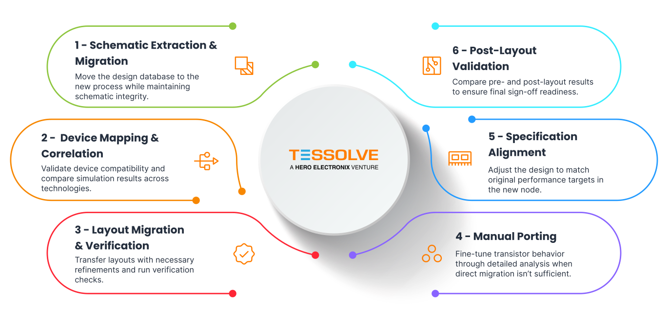
How We Work
Technology migration isn’t just about moving data from one node to another. It’s about preserving
performance, intent, and reliability while adapting to a new process.
At Tessolve, we follow a structured six-step approach that ensures every design is carefully validated,
aligned, and optimized, delivering silicon that is ready for manufacturing in the destination technology.
Analog & Mixed-Signal (AMS)
Custom analog and mixed-signal design from concept to silicon[SK3.1]
Tessolve delivers end-to-end analog and mixed-signal (AMS) design services, spanning specification, design, layout, signoff, and post-silicon validation across both mature and advanced process nodes.
Highlights
- Complete AMS design lifecycle ownership
- Block-level and full-chip IP development
- Proven delivery on CMOS and FinFET technologies
- End-to-end responsibility from specs to GDSII
Process Nodes Supported
3nm | 5nm | 7nm | 10nm | 14nm | 22nm | 45nm | 65nm | 90nm | 130nm | 180nm | 350nm
Industry Experience
Automotive | Communications | Consumer | Medical | IoT
Know More
Brochure PDF Download
RTL Design
Scalable RTL development and SoC integration
Tessolve provides RTL design services for IP and SoC development, with a focus on large-scale integration and quality, power, and performance.
Highlights
- Standard and complex IP block development
- SoC and subsystem integration, clock/reset design
- Low-power RTL design with UPF
- RTL quality checks: Lint, CDC, low-power checks
- Protocol expertise: PCIe, USB, MIPI, AMBA, DDR, I2C, SPI, UART
Design Verification
Sector-agnostic verification across IPs and SoCs
Tessolve provides comprehensive design verification services to ensure functional correctness, coverage closure, and quality across IP and SoC designs. Our teams use proven methodologies and tools to manage verification complexity, reduce risk, and support predictable tape-out schedules.
Highlights
- Standard and complex IP block development
- SoC and subsystem integration, clock/reset desig
- Low-power RTL design with UPF
- RTL quality checks: Lint, CDC, low-power checks
- Protocol expertise: PCIe, USB, MIPI, AMBA, DDR, I2C, SPI, UART
Design Verification
Brochure PDF Download
RISC-V Test and
Verification Solutions
Design for Test (DFT)
Improving test coverage and silicon quality
Tessolve provides comprehensive DFT services to enhance testability, yield, and first-pass silicon success, supported by strong post-silicon debug capabilities.
Highlights
- DFT architecture and scan methodology
- RTL-level DFT quality checks
- Scan insertion, ATPG generation, and verification
- Memory BIST and boundary scan
- Fault coverage analysis and post-silicon debug support
About DFT
Brochure PDF Download
Design for Test/Debug (DFT/DFD)
Physical Design
From netlist to tape-out-ready layout
Tessolve delivers end-to-end physical design services, transforming front-end designs into optimized layouts that meet timing, power, and area goals.
Highlights
- Mixed-signal SoC execution from spec to silicon
- Expertise in complex IPs and high-performance subsystems
- Timing closure for designs up to 3GHz
- Advanced-node support down to 3nm
- Low-power implementation and signoff readiness
Know More
Brochure PDF Download
FPGA & Emulation
Early validation through prototyping and emulation
Tessolve enables early hardware validation using FPGA prototyping and emulation to accelerate system debugging and software
Highlights
- Experience with AMD and Intel FPGA platforms
- FPGA-based emulation and design partitioning
- Custom Silicon-to-FPGA and FPGA-to-Custom Silicon conversion
- Custom board development and FPGA validation
Foundry Porting Services
Reliable migration across process nodes and foundries
Tessolve enables seamless porting of existing VLSI designs to new technologies or foundries while preserving original functionality, performance, and specifications. Our structured and automation-driven approach ensures predictable outcomes with minimal risk.
Highlights
- Schematic, layout, and testbench migration across source and target foundries
- Parameter and device mapping across heterogeneous PDKs
- Automated scripting to handle symbol, model, and rule differences
- Reusable porting flows for faster turnaround on repeat migrations
- Full functional and performance verification post-migration
Porting Methodology
- Adaptation of schematics and layouts to target process design rules
- Script-based translation of parameters, symbols, and model references
- Integration with target foundry model files and simulation setup
- Comprehensive verification to ensure spec and functional equivalence
Why Choose Tessolve
1250+ VLSI engineers delivering complete Spec-to-GDSII solutions with integrated post-silicon support
Proven execution across 350nm to advanced 2nm nodes, including CMOS and FinFET technologies
70+ silicon-proven analog designs and multiple mixed- signal SoCs delivered to global customers
Turnkey capabilities spanning architecture, RTL, verification, DFT, physical design, and validation
FAQs
1. What is IC design and what does the process involve?
IC design is the process of developing an integrated circuit from functional requirements through architecture, circuit or RTL design, verification, physical implementation, and final sign-off. The flow is optimized for factors such as performance, power, area, timing, and reliability.
2. What are the main stages of IC design?
The IC design flow typically includes specification and architecture, RTL or circuit design, functional verification, synthesis, DFT, physical design, timing and physical sign-off, and GDSII generation.
3. What is Spec-to-GDSII in IC design?
Spec-to-GDSII covers the IC development flow from defining the architecture and implementing the design through verification, physical design, sign-off, and generation of the GDSII database required for fabrication.
4. How do advanced semiconductor process nodes affect IC design?
Smaller process nodes increase transistor density but also introduce tighter design rules, greater routing and timing complexity, increased process variability, and more demanding power and signal-integrity requirements. Advanced-node designs therefore require rigorous verification and physical sign-off.
5. What types of IC designs does Tessolve support?
Tessolve supports analog, digital, and mixed-signal IC design, including IPs, subsystems, and complex SoCs across a range of semiconductor applications.
6. What IC Design Services does Tessolve provide?
Tessolve provides end-to-end IC Design Services covering architecture, RTL design, verification, DFT, synthesis, physical design, and GDSII sign-off, with IC design engineering experience across process technologies from 2nm to 350nm.
7. Does Tessolve support IC design beyond the tape-out stage?
Yes. Tessolve extends its semiconductor engineering capabilities into post-silicon validation, including silicon bring-up, functional validation, characterization, debug, and performance and power analysis.
8. How does IC verification contribute to successful silicon?
IC verification identifies functional, timing, power, and integration issues before fabrication. Techniques such as simulation, formal verification, coverage analysis, and gate-level verification reduce design risk and the likelihood of costly silicon re-spins.
9. What is DFT and why is it important in IC design?
Design-for-Test (DFT) incorporates test structures into an IC to make manufacturing defects easier to detect and diagnose. Techniques such as scan, ATPG, MBIST, and boundary scan improve test coverage and chip testability.