
Reducing re-spins in ultra-fine pitch designs through disciplined, manufacturing-aware design
Designing PCBs with <0.35 mm pitch BGAs pushes layout and manufacturing capability to their limits. At this scale, even small deviations in pad geometry, via design, solder mask registration, or routing tolerance can lead to assembly defects, reliability risks, costly re-spins, and schedule delays.
That is why Design for Manufacturability (DFM) must guide decisions from the earliest stages of stack-up planning, breakout strategy, footprint creation, and assembly definition, rather than being treated as a final verification step.
This article outlines the DFM strategies that matter most for reducing re-spins and improving manufacturability in ultra-fine pitch BGA designs.
Why <0.35 mm Pitch BGA Designs Are So Challenging
- Escape routing space becomes extremely limited
- Microvia and HDI decisions directly affect yield and reliability
- Fabrication capability gaps quickly turn into expensive re-spins
- Solder mask alignment tolerance becomes critical
- Small footprint or paste design errors can cause bridging or opens
The following DFM priorities have the greatest impact on yield, reliability, and first-pass success.
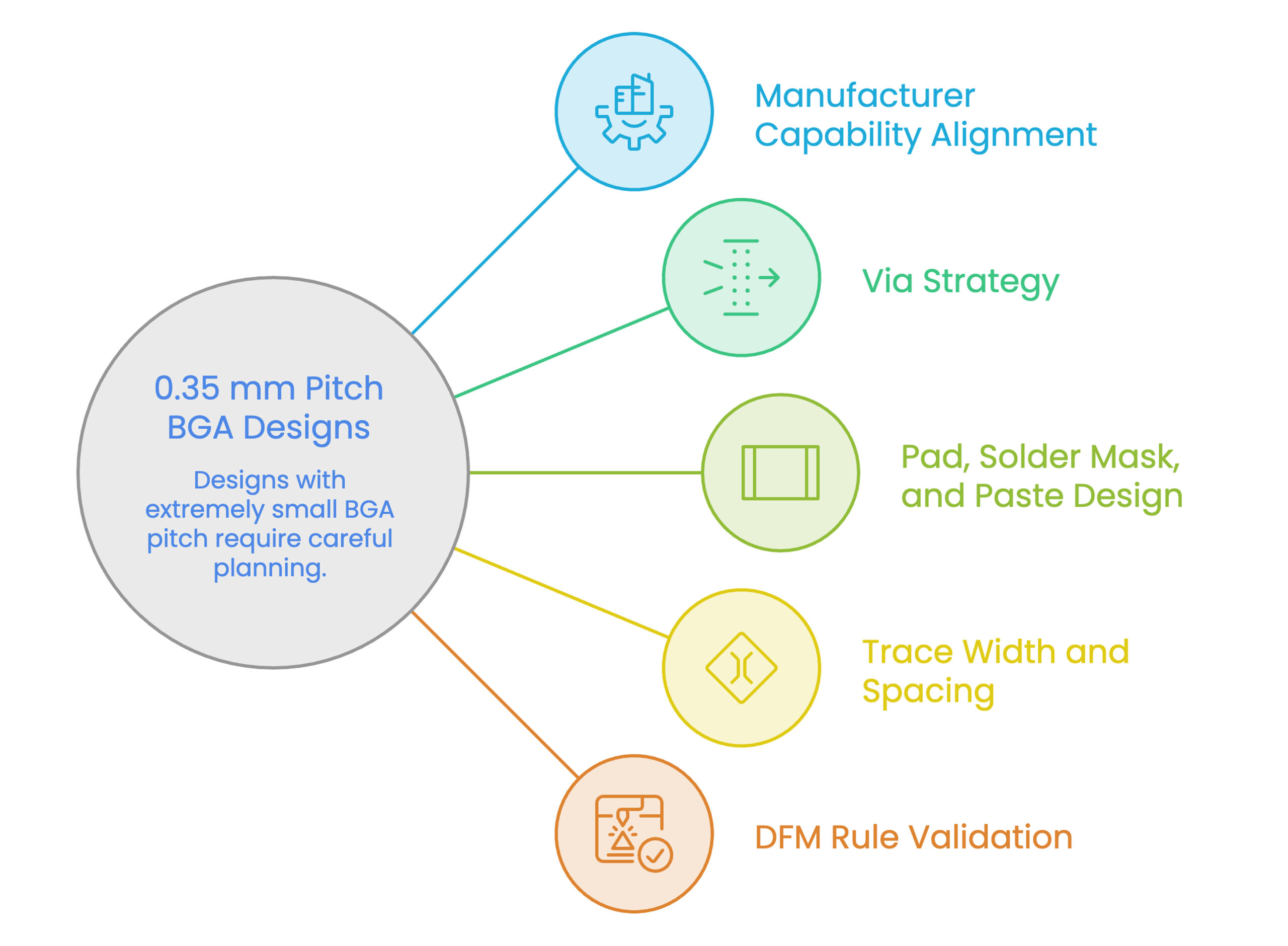
1. Start with Manufacturer Capability Alignment
In ultra-fine pitch BGA designs, the PCB manufacturer is effectively part of the design team. If the design assumptions exceed proven fabrication or assembly capability, failure risk rises sharply.
Key Challenges
- Minimum trace and spacing capability
- Laser-drilled microvia process limits
- Sequential lamination constraints
- Via fill, cap, and planarization capability
Recommended Actions
- Review the fabricator’s capability matrix before layout begins
- Align pad, via, and routing rules to proven process limits
- Confirm stack-up assumptions early
- Validate assembly expectations along with fabrication limits
Best Practice
- Freeze manufacturer-approved rules before detailed breakout work starts
2. Use the Right Via Strategy
At <0.35 mm pitch, conventional through-hole escape routing is often impractical. Via strategy becomes a primary driver of routability, cost, and long-term reliability.
Common Via Strategies
Microvias
Microvias are the preferred escape solution for fine-pitch BGAs because they reduce pad size requirements and support dense fanout.
Advantages
- Smaller capture pads – Improved breakout density
- Reduced electrical stub effects
- Better support for HDI stack-ups
Considerations
- Aspect ratio limits
- Reliability of stacked structures
- Copper filling and planarization quality
Via-in-Pad with Filled and Capped Microvias
Via-in-pad with filled and capped microvias is often necessary when routing channels are extremely limited and direct pad escape is the only practical solution.
Benefits
- Maximum routing density
- Shorter interconnect paths
- Better high-speed electrical performance
Challenges
- Higher fabrication cost
- Strict fill and planarization requirements
- Assembly sensitivity if via filling is inconsistent
3. Optimize BGA Pad, Solder Mask, and Paste Design
At ultra-fine pitch, pad and paste design directly influence assembly yield. Minor geometry errors can quickly translate into bridging, opens, or weak solder joints.
Critical Areas
BGA Pad Size
Pad dimensions must align with supplier guidance, IPC recommendations, and proven assembly capability.
Solder Mask Strategy
Below 0.35 mm pitch, solder mask registration becomes highly sensitive, so NSMD versus SMD selection must be based on actual process capability and reliability goals.
Solder Paste Aperture Optimization
Stencil design often needs aperture reduction or modified aperture shapes to manage paste volume and reduce bridging risk.
Potential Assembly Defects
- Solder bridging
- Insufficient solder volume
- Voiding
- Adjacent passive disturbance during reflow
4. Control Trace Width and Spacing Inside the BGA
Routing within a sub-0.35 mm BGA is highly constrained. Every neck-down, clearance, and escape decision affects manufacturability as much as routability.
Design Challenges
- Limited breakout channels
- Tolerance accumulation in ultra-fine features
- Acid trap risk from poor routing geometry
- Yield loss when all dimensions are pushed to minimum simultaneously
Strategy Recommendations
- Use fabricator-approved trace and spacing rules
- Minimize unnecessary neck-downs
- Prefer 45° routing and clean escape geometry
- Validate signal integrity and return path continuity early
5. Validate DFM Rules Before Release
Passing internal CAD checks does not prove manufacturability. Advanced BGA designs require dedicated DFM validation before fabrication data is released.
Essential Validation Areas
Fabrication Checks
- Annular ring and drill-to-copper clearance
- Via aspect ratio and fill capability
- Copper balancing and etch risk
- Solder mask sliver and alignment risk
Assembly Checks
- Paste-to-pad alignment
- Bridging risk at fine pitch sites
- Via-in-pad process validation
- Component spacing and stencil manufacturability
Reliability Checks
- Microvia stacking limits
- Thermal stress concentration areas
- Copper density imbalance
- Long-term reliability of HDI structures
Recommended Workflow
Before release:
- Share stack-up and breakout assumptions with the fabricator
- Validate HDI and assembly capability together
- Review the DFM report jointly
- Confirm stencil and paste assumptions
- Freeze approved design rules before data release
Why Tessolve Is a Strong Partner for Ultra-Fine Pitch PCB Design
Ultra-fine pitch BGA design demands more than advanced layout capability. It requires disciplined DFM execution, deep HDI expertise, and early alignment between design, fabrication, and assembly.
At Tessolve, we bring these capabilities together through strong PCB design and engineering expertise, manufacturing-aware design practices, and close collaboration with fabrication and assembly partners. Our teams work across stack-up planning, breakout strategy, HDI design, footprint validation, and DFM review to reduce re-spins and improve first-pass success.
With experience in complex, high-density PCB development, Tessolve helps customers balance electrical performance, manufacturability, reliability, and program timelines from the earliest stages of design.
The result is a more robust path to production: fewer design iterations, higher yield, and greater confidence in ultra-fine pitch designs from prototype through volume manufacturing.
Frequently Asked Questions (FAQs)
1. Why do ultra-fine pitch PCB designs often require multiple re-spins?
Ultra-fine pitch PCB designs often require multiple re-spins because tiny errors in spacing, routing, or footprints can easily cause manufacturing or assembly failures at such tight tolerances.
2. What is the biggest DFM mistake designers make in 0.15mm pitch PCBs?
Designing beyond manufacturer capabilities without validation often leads to failed fabrication and costly design iterations.
3. How can I reduce solder bridging in fine-pitch PCB designs?
Optimize solder mask clearance, adjust stencil apertures, and ensure proper component spacing to prevent excess solder deposition.
4. Are microvias necessary for ultra-fine pitch PCB layouts?
In most cases, yes. They help achieve higher routing density, but should be used carefully to avoid added complexity.
5. When should DFM checks be performed during PCB design?
Ideally, from the early design stage and continuously throughout, not just as a final step before manufacturing.