
Semiconductor process nodes are the foundation of modern chip manufacturing, defining how small and efficient transistors on a chip can be. As technology advances, these nodes have evolved from larger geometries to ultra-small scales like 7nm, 5nm, and now 2nm. Understanding 7nm vs 5nm vs 2nm is crucial because each node directly impacts chip performance, power consumption, manufacturing complexity, and production cost.
In today’s competitive landscape, selecting the right node is no longer just a technical decision; it’s a strategic one. A smaller node can deliver higher performance and better energy efficiency, but it also increases design complexity and manufacturing expenses. This trade-off becomes especially important in industries like AI, mobile devices, and automotive electronics, where performance and efficiency are key differentiators.
As shrinking nodes continue to shape innovation across sectors, businesses and engineers must carefully evaluate their options. This guide will help you compare different process nodes and make informed decisions based on your specific design and application requirements.
What is a Semiconductor Process Node?
A semiconductor process node refers to a specific generation of manufacturing technology used to fabricate integrated circuits. In earlier days, node names such as 90nm or 45nm directly indicated the physical dimensions of transistor features, particularly the gate length. However, in today’s advanced technologies, node naming has become more of a branding convention rather than an exact measurement.
Over time, the industry has evolved from micron-scale manufacturing to nanometer-scale precision, enabling billions of transistors to be integrated onto a single chip. This evolution has significantly enhanced chip capabilities and efficiency.
Key parameters influenced by process nodes include:
- Transistor Density: Smaller nodes allow more transistors within the same chip area, improving functionality and integration.
- Power Consumption: Reduced transistor size lowers power usage, making chips more energy-efficient.
- Performance: Higher density and faster switching speeds lead to improved computational performance.
For any VLSI design company, understanding these factors is essential for optimizing chip performance and meeting modern design requirements.
It’s important to note that node names like 7nm or 5nm no longer represent exact physical gate lengths but rather indicate relative technological advancement and efficiency improvements.
Evolution of Advanced Nodes: From 7nm to 2nm
The progression from 7nm to 2nm marks one of the most significant advancements in semiconductor manufacturing, driven by the growing demand for higher computing performance, greater transistor density, and improved power efficiency. Leading foundries such as TSMC, Samsung Electronics, and Intel continue to push the boundaries of process technology to support next-generation applications.
The transition from 7nm to 5nm delivered substantial improvements in performance-per-watt and transistor density. Moving to 2nm, manufacturers are introducing even more advanced transistor architectures and manufacturing techniques to overcome the physical limitations of traditional scaling and enable greater computational capabilities.
Some key technological shifts include:
- FinFET Technology (7nm & 5nm): A 3D transistor structure that improved control over current flow and reduced leakage.
- GAAFET/Nanosheet Technology (2nm): The latest 2nm process nodes adopt Gate-All-Around (GAAFET) or nanosheet transistor architectures, providing superior electrostatic control, lower leakage currents, and higher performance with improved power efficiency.
Alongside these advancements, manufacturing complexity has increased significantly. Advanced lithography techniques such as EUV are now essential, making production more expensive and technically demanding.
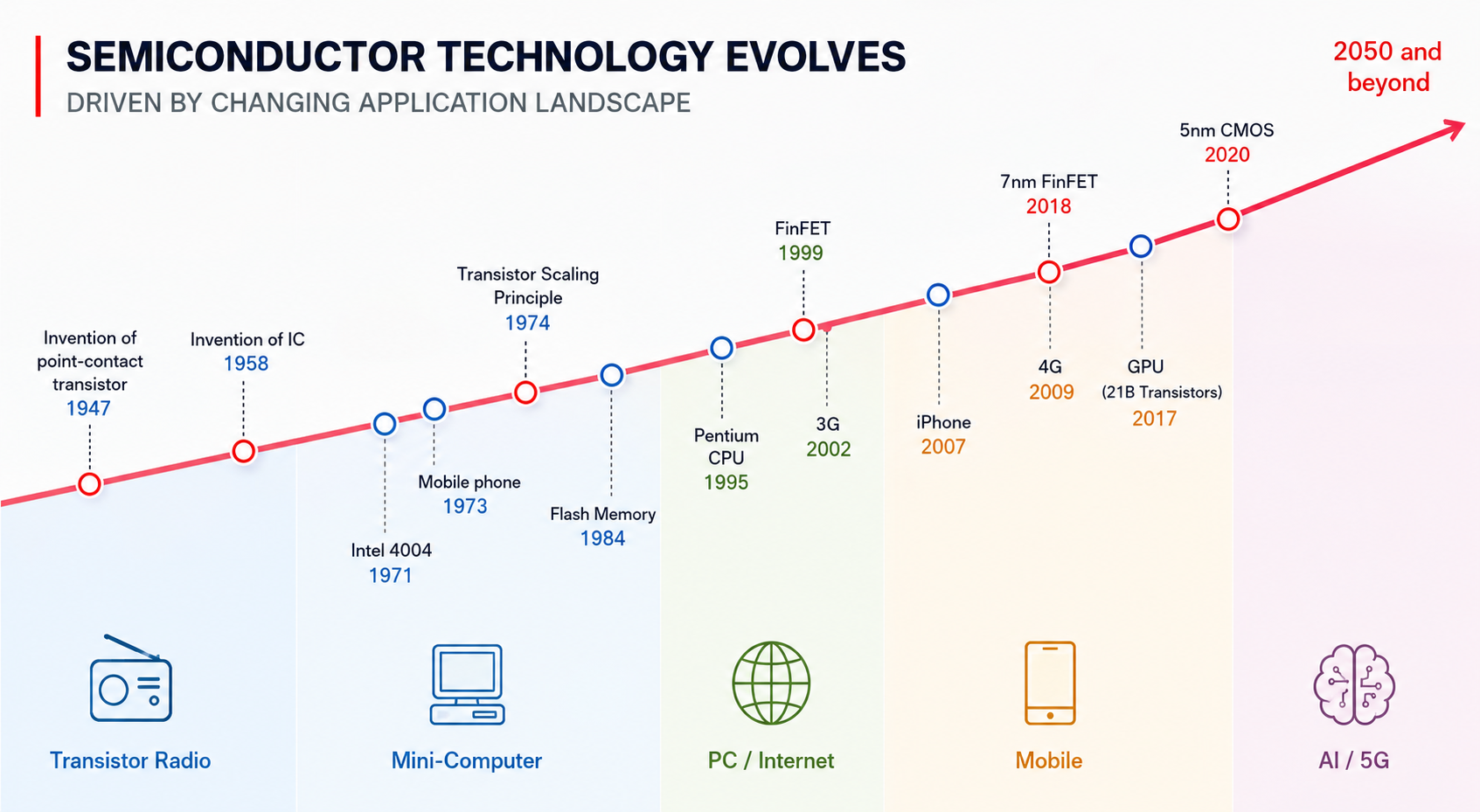
A proper semiconductor process node comparison shows that while each new node offers performance benefits, it also introduces trade-offs in cost, yield, and design complexity. The evolution of semiconductor nodes is best understood through a visual timeline. The infographic below highlights key milestones that led to today’s advanced technologies:
How Do the Advanced Digital Process Nodes Contribute to Semiconductor Test Innovations?
7nm Technology: Features, Pros, and Limitations
The 7nm process node is considered a mature and reliable technology in today’s semiconductor ecosystem. It offers a balanced combination of performance, power efficiency, and cost, making it widely adopted across multiple industries.
Key Features:
- Mature fabrication process with stable manufacturing ecosystems
- Good balance between performance and cost efficiency
Advantages:
- Lower manufacturing cost compared to newer nodes
- Higher yield rates due to process maturity
- Easier design implementation for many applications
Limitations:
- Lower transistor density compared to 5nm and 2nm
- Higher power consumption relative to advanced nodes
- Not ideal for cutting-edge, high-performance workloads
Typical Use Cases:
- Automotive electronics requiring long-term reliability
- Industrial control systems
- Mid-range processors and consumer devices
For organizations involved in VLSI chip design, 7nm remains a practical choice when cost efficiency and stability are more critical than achieving the highest possible performance.
5nm Technology: Features, Pros, and Limitations
The 5nm process node represents a significant advancement over 7nm, delivering improved performance and energy efficiency. It is widely used in modern high-performance applications, especially in flagship consumer devices.
Key Improvements Over 7nm:
- Approximately 1.8x higher transistor density
- Enhanced power efficiency and faster processing speeds
Advantages:
- Strong performance-per-watt, ideal for energy-sensitive applications
- Widely adopted in premium smartphones and advanced processors
- Enables compact and powerful chip designs
Limitations:
- Higher manufacturing and development costs
- Increased design complexity requires advanced expertise
- More challenging verification and validation processes
Use Cases:
- Smartphones and premium mobile devices
- AI accelerators and machine learning chips
- High-performance computing systems
Many advanced semiconductor node design companies prefer 5nm for its ability to balance efficiency and performance, making it a go-to choice for next-generation products.
2nm Technology: Features, Pros, and Limitations
The 2nm process node represents the latest generation of semiconductor manufacturing, delivering unprecedented levels of transistor density, power efficiency, and computing performance. Designed for the most demanding workloads, it enables the development of next-generation AI processors, high-performance computing systems, premium mobile chipsets, and advanced automotive platforms.
Cutting-Edge Innovations:
- GAAFET/Nanosheet Architecture: Unlike the FinFET architecture used in 7nm and 5nm technologies, 2nm nodes leverage Gate-All-Around (GAAFET) or nanosheet transistors to provide better channel control, significantly reducing leakage current and improving switching performance.
Advantages:
- Exceptional processing performance for compute-intensive applications
- Industry-leading power efficiency with lower energy consumption
- Highest transistor density, allowing greater functionality within a smaller chip area
- Better thermal characteristics for advanced AI and HPC workloads
Limitations:
- Extremely high fabrication and development costs
- Limited foundry availability due to cutting-edge manufacturing requirements
- Highly complex design, verification, and packaging processes
- Longer development cycles compared to mature nodes
Use Cases:
- Next-generation processors
- Advanced AI and machine learning accelerators
- High-performance computing (HPC)
- Premium smartphones and laptops
- Intelligent automotive computing platforms
While 2nm delivers the highest level of semiconductor innovation currently available, it is best suited for applications where maximum performance, efficiency, and transistor density justify the increased development and manufacturing costs.
7nm vs 5nm vs 2nm: Detailed Comparison
To better understand the differences between these process nodes, the table below highlights how each generation compares across key design and manufacturing parameters.
| Feature | 7nm | 5nm | 2nm |
| Transistor Density | Medium | High | Extremely High |
| Power Efficiency | Good | Better | Best |
| Performance | Good | High | Exceptional |
| Cost | Lower | High | Extremely High |
| Maturity | Mature | Mature | Early Adoption |
| Transistor Architecture | FinFET | FinFET | GAAFET / Nanosheet |
| Typical Use Cases | Automotive, Industrial | Mobile, AI | AI, HPC, Premium Mobile |
This comparison shows that each process node offers unique advantages based on application requirements. While 7nm remains a cost-effective and reliable choice, 5nm provides an excellent balance of performance and efficiency. 2nm leads in transistor density and power efficiency but also comes with significantly higher development and manufacturing costs.
For businesses evaluating 7nm vs 5nm vs 2nm, the right choice depends on performance needs, budget, product lifecycle, and time-to-market rather than simply choosing the smallest process node.
Key Factors to Consider When Choosing a Process Node
Choosing the right semiconductor process node requires a careful evaluation of multiple technical and business factors. Each project has unique requirements, and selecting the wrong node can impact both performance and profitability.
When making a decision, consider the following:
- Performance Requirements: Applications like high-performance computing and AI demand maximum speed and processing power, making advanced nodes more suitable. Standard applications may perform well on mature nodes like 7nm.
- Power Efficiency: For battery-powered devices such as smartphones and IoT systems, energy efficiency is critical. Smaller nodes, like 5nm and 2nm, provide significant advantages in reducing power consumption.
- Cost Constraints: Budget plays a major role in node selection. Advanced nodes come with higher fabrication and design costs, so it’s important to evaluate return on investment before choosing them.
- Time to Market: Mature nodes typically have well-established manufacturing processes, allowing faster production and deployment compared to newer nodes.
- Design Complexity: As nodes shrink, design and verification become more complex. This requires skilled teams and advanced tools, often increasing development time and cost.
- Application Type: Different industries have different priorities. Automotive and industrial sectors prioritize reliability, while consumer electronics and AI focus on performance and efficiency.
A structured semiconductor process node comparison helps organizations align their technical goals with business strategy, ensuring the right balance between innovation and practicality.
Real-World Applications and Industry Trends
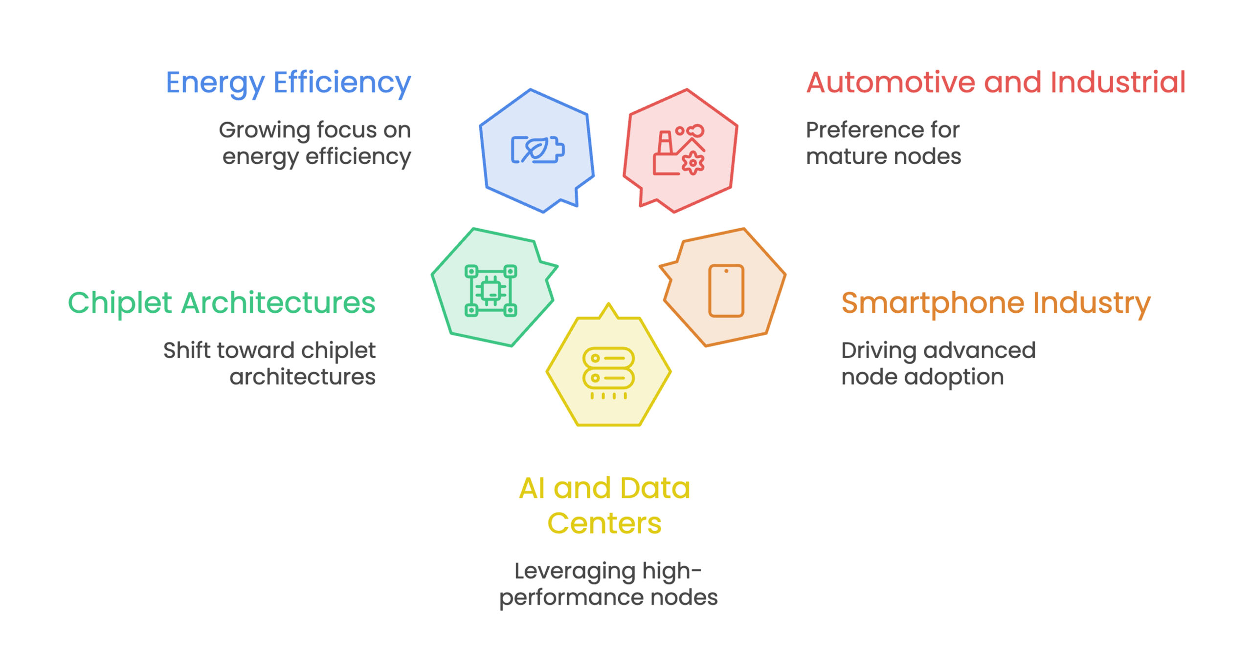
The adoption of semiconductor nodes varies across industries, depending on priorities such as performance, efficiency, and reliability. Several key trends highlight how different sectors approach node selection:
- Automotive and Industrial Preference for Mature Nodes: Industries like automotive and industrial systems prioritize reliability, long lifecycle support, and safety. This makes 7nm and similar mature nodes a practical choice over cutting-edge technologies.
- Smartphone Industry Driving Advanced Node Adoption: Mobile manufacturers rapidly adopt 5nm and 2nm nodes to deliver faster processors, improved battery life, enhanced AI capabilities, and compact device designs in premium smartphones.
- AI and Data Centers Leveraging High-Performance Nodes: AI accelerators, cloud infrastructure, and high-performance computing platforms increasingly rely on 5nm and 2nm technologies to support massive computational workloads while maximizing energy efficiency.
- Shift Toward Chiplet Architectures: Instead of relying solely on monolithic chips, companies are increasingly using chiplet-based designs to improve scalability and manage costs effectively.
- Growing Focus on Energy Efficiency: Across industries, there is a strong push toward reducing power consumption, driven by sustainability goals and the need for efficient large-scale computing.
These trends show how node selection is closely tied to application-specific demands and evolving technological priorities.
Challenges in Advanced Node Adoption
Despite their advantages, advanced semiconductor nodes introduce several challenges that organizations must address during adoption:
- Rising Fabrication Costs: Manufacturing at 5nm and especially 2nm requires multi-billion-dollar investments in advanced fabrication facilities, EUV lithography, and cutting-edge process technologies, making production feasible for only a handful of global foundries.
- Yield and Manufacturing Complexity: As transistor sizes shrink, maintaining consistent yields becomes more difficult, leading to potential production inefficiencies and increased waste.
- Increased Design and Verification Complexity: Advanced nodes demand highly sophisticated design tools and expertise, as engineers must manage tighter tolerances and new physical effects.
- Limited Foundry Availability: Only a few manufacturers have the capability to produce chips at advanced nodes, creating supply constraints and potential delays.
- Supply Chain Challenges: Global semiconductor supply chains can impact the availability of materials, equipment, and manufacturing capacity, affecting timelines and costs.
These challenges emphasize the need for strategic planning and technical expertise when working with advanced semiconductor technologies.
Make the Right Process Node Choice with Tessolve’s Expertise
Tessolve understands that choosing between 7nm, 5nm, and 2nm is more than a technical decision; it’s a critical step in defining your product’s success. With our deep expertise in semiconductor engineering and end-to-end design services, we help you evaluate the right process node based on performance goals, power efficiency, and cost constraints. From concept to silicon, our team works closely with you to simplify complex design challenges and accelerate time-to-market. Whether you’re targeting mature nodes for reliability or advanced nodes for innovation, we ensure your solution is optimized, scalable, and future-ready. Let’s build smarter, more efficient chips together.
Frequently Asked Questions (FAQs)
1. What is the main difference between 7nm, 5nm, and 2nm process nodes?
The primary difference lies in transistor density, power efficiency, performance, and manufacturing complexity. 2nm offers the highest efficiency and computational performance, while 7nm remains a mature, reliable, and cost-effective option for many applications.
2. Is 2nm always better than 5nm for every application?
Not necessarily. While 2nm delivers superior performance and power efficiency, it also comes with significantly higher costs and design complexity. For many products, 5nm continues to provide the ideal balance between performance, efficiency, and manufacturing cost.
3. Why are smaller semiconductor nodes more expensive to manufacture?
Advanced nodes require cutting-edge equipment like EUV lithography, complex design processes, and higher R&D investments, significantly increasing fabrication costs compared to mature nodes like 7nm.
4. Which process node is best suited for automotive applications?
Automotive applications typically prefer mature nodes like 7nm due to their proven reliability, longer lifecycle support, and cost efficiency rather than adopting the latest, more complex nodes.
5. How does process node size impact battery life in devices?
Smaller nodes like 5nm and 2nm improve power efficiency by reducing energy consumption and leakage current, helping extend battery life in smartphones, laptops, wearables, and other portable electronic devices.