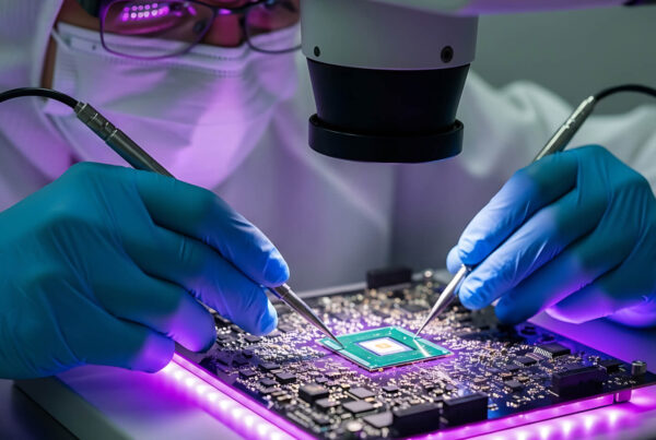

As technology continues to evolve, the competition to produce increasingly complex devices that enhance customers’ lives grows. To meet this demand, manufacturers require more advanced processing nodes and chips to deliver better performance.
The ongoing advancements in semiconductor devices are continually pushing the limits of what is achievable. The introduction of advanced digital process nodes, particularly those smaller than 10 nanometers (nm), has transformed the semiconductor industry. These smaller nodes allow for the integration of more transistors, resulting in improved performance and greater complexity in devices. However, these advancements also present unique challenges when it comes to testing these intricate circuits.
In this blog, we will explore how advanced digital process nodes are driving innovations in semiconductor testing. Additionally, we will highlight how the development of these advanced nodes has enabled Tessolve, a leading semiconductor company in the USA, to enhance its testing capabilities.
How Advanced Digital Process Nodes Contribute to Semiconductor Test Innovations
Let’s explore the contribution of the advanced digital process nodes in semiconductor test innovation.
Increased Device Complexity
Advanced digital process nodes enable the integration of a significantly higher number of transistors within smaller chip areas. Modern SoCs now combine CPUs, GPUs, AI accelerators, memory controllers, security modules, and high-speed interfaces into a single package.
While this enhances functionality and computational capability, it also increases testing complexity. Semiconductor test innovations now rely on AI-assisted fault diagnostics, advanced Design-for-Test (DFT) methodologies, scan compression techniques, and automated test pattern generation (ATPG) to accurately identify defects and ensure device reliability.
Higher Performance and Operating Speeds
Modern semiconductor devices operate at extremely high frequencies with tighter timing margins. Advanced nodes are designed to support applications such as 5G, AI, edge computing, and high-performance data centers that demand ultra-fast processing speeds.
Testing these devices requires highly accurate validation techniques. Semiconductor test innovations now focus on high-speed functional testing, at-speed scan testing, jitter analysis, and timing-aware validation methodologies to ensure chips meet stringent performance and reliability requirements.
Signal Integrity and Power Integrity Challenges
As transistor geometries continue shrinking, maintaining signal integrity becomes increasingly difficult. Crosstalk, electromagnetic interference, IR drop, leakage current, and power noise become more critical in advanced nodes.
To address these issues, semiconductor testing now includes advanced power integrity analysis, high-speed signal validation, SI/PI simulations, and low-voltage stress testing. These innovations help improve overall chip stability, reliability, and operational consistency.
Manufacturing Variability and Yield Optimization
Advanced process nodes introduce higher manufacturing variability due to increasingly complex fabrication processes such as EUV lithography, FinFET, and Gate-All-Around (GAA) transistor architectures.
Semiconductor test innovations leverage statistical analysis, adaptive test methodologies, Built-In Self-Test (BIST), machine learning-driven analytics, and predictive yield optimization to identify process variations early and improve manufacturing yield.
Test Cost and Time Reduction
As chip complexity increases, semiconductor testing costs also rise due to longer test times and sophisticated test equipment requirements. Reducing test cost while maintaining high fault coverage has become a major priority for semiconductor companies.
Modern semiconductor testing addresses this challenge through parallel testing, test time optimization, smart binning techniques, automated debugging, and improved fault coverage algorithms. These innovations help reduce production costs while ensuring high-quality chip validation.
Role of DFT in Designing High-Quality PCB
Innovative Test Innovation at Tessolve Powered by Advanced Digital Process Nodes
In the fast-paced world of semiconductor testing, Tessolve has emerged as a pioneer, leveraging the profound impact of advanced digital process nodes to fuel its innovation. By embracing the cutting-edge technologies offered by these nodes, Tessolve has redefined the boundaries of semiconductor testing, leading to breakthroughs and unmatched efficiency.
Advanced digital process nodes have opened up a new realm of possibilities for Tessolve. These nodes have revolutionized the semiconductor landscape with smaller transistor sizes, increased density, and improved power efficiency. Tessolve’s engineers can now design and implement once inconceivable and highly sophisticated test methodologies.
The impact is twofold: enhanced performance and reduced costs. The superior capabilities of advanced digital process nodes allow Tessolve to deliver more accurate and reliable test results, ensuring the highest quality standards. The smaller form factor and lower power consumption also enable greater test integration and higher throughput, resulting in significant cost savings for clients.
Conclusion
Tessolve’s commitment to semiconductor test innovations has been instrumental in establishing it as a semiconductor leader in the USA. The impact of advanced digital process nodes empowers Tessolve to provide comprehensive and cutting-edge semiconductor test innovations. By harnessing the power of advanced digital process nodes, Tessolve has cemented its position as an industry leader, driving semiconductor test innovation to new heights. The convergence of technology and expertise has created a transformative synergy, propelling the industry forward and enabling the development of even more advanced and efficient electronic devices.
FAQs
1. What are advanced process nodes in semiconductormanufacturing?
Advanced process nodes refer to smaller semiconductor fabrication technologies, such as 5nm and 3nm, that improve chip performance, efficiency, and transistor density.
2. What is a process node in semiconductortechnology?
A process node represents the manufacturing technology used to fabricate semiconductor chips, typically measured in nanometers (nm).
3. How do advanced semiconductor nodes improve chip performance?
Advanced nodes enable faster processing speeds, lower power consumption, higher transistor density, and improved overall chip efficiency.
4. What challenges do advanced process nodes create for semiconductor testing?
Advanced nodes increase testing complexity due to signal integrity issues, manufacturing variability, power leakage, and higher operating frequencies.
5. Which industries benefit the most from advanced semiconductor process nodes?
Industries including AI, 5G, automotive, consumer electronics, IoT, cloud computing, and data centers benefit significantly from advanced nodes.