
Design cycles are getting shorter, SoCs are getting more complex, and the definition of “done” is shifting. Today, implementing Design-for-Test (DFT) at the end of RTL development simply doesn’t work. Teams are now embracing a parallel approach, where design and test planning evolve together. This shift toward early DFT integration enables smoother implementation, higher coverage, and fewer surprises during silicon bring-up.
So, what’s really driving this change? The answer is simple: efficiency, predictability, and first-pass silicon success.
Why Early DFT Matters
Traditionally, DFT insertion came late in the flow, often after synthesis. But the challenge with this approach is that test logic interacts with RTL in ways that can disrupt timing and functional behavior. Making changes late leads to rework, delays, and additional debug cycles.
Integrating DFT during RTL development allows teams to evaluate controllability, observability, scan architecture, and test access points upfront. When teams collaborate early, including RTL engineers, verification engineers, and those specializing in test engineering, the results are remarkably smoother.
This approach also ensures that strategies like Built-In Self-Test (BIST), scan compression, and hierarchical test methodologies are considered before physical constraints lock the design.
Technical Advantages of Early DFT Integration
When DFT is embedded early instead of patched in later, several tangible benefits emerge:
1. Better Fault Coverage With Less Rework
Test structures added with functional context enable efficient ATPG and improve defect detection rates. This accelerates semiconductor testing workflows both pre- and post-silicon.
2. Faster and Cleaner Timing Closure
Designers can optimize timing budgets early to prevent last-minute timing failures caused by scan chain routing.
3. Parallel Development
DFT readiness allows test teams to begin pattern development and validation in parallel, as the RTL matures, boosting productivity and accelerating test engineering cycles.
4. Optimized Architectures for Complex Systems
With early planning, SoC Testing infrastructures such as TAP controllers, IEEE 1500 wrappers, and test buses are defined during SoC organization, not after everything is assembled.
Practical Steps to Adopt Concurrent RTL + DFT Planning
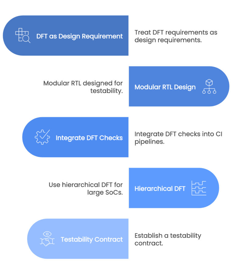
Moving DFT earlier doesn’t happen automatically; it requires clear processes. Here are the steps leading companies now follow:
1. Treat DFT Requirements as Design Requirements
Scan, BIST, JTAG, and compression techniques must be clearly documented in the design specification, not treated as enhancements.
2. Modular RTL Designed for Testability
Clock-gating strategies, register implementations, and boundary logic should be written with test access in mind.
3. Integrate DFT Checks into CI Pipelines
Automated scripts and early ATPG feasibility analysis flag issues before synthesis, accelerating semiconductor testing validation and reducing debug loops.
4. Use Hierarchical DFT for Large SoCs
Testing at the IP level ensures easier debugging and makes SoC Testing scalable.
5. Establish a Testability Contract
Shared RTL conventions make integration seamless across teams, vendors, and development sites.
The Human Element: Culture Shift Required
Tools and processes are essential, but collaboration is the real catalyst.
- RTL designers must understand test constraints and scan-friendly design practices.
- Verification teams should validate test modes alongside functional modes.
- Test engineers should be involved during architecture, not after sign-off.
As organizations blend responsibility across roles, test engineering becomes a strategic function, not just a downstream checkpoint.
This culture shift also encourages documentation discipline, design reviews that include test intent, and continuous alignment between hardware, verification, and manufacturing stakeholders.
How It Impacts Silicon Validation and Manufacturing
Early DFT significantly improves downstream readiness. Once silicon arrives, teams leveraging early planning experience:
- Faster debug cycles
- More predictable bring-up timelines
- Faster yield learning and reliability improvements
That’s because the hooks required for fault localization, observability, and pattern debugging were considered early, not retrofitted.
This is especially important in industries where reliability is non-negotiable, automotive, networking, AI compute, and aerospace, where semiconductor testing rigor and compliance practices shape everything from safety certifications to customer acceptance.
Trends Accelerating This Shift
The momentum behind early DFT integration continues to grow due to:
- AI-assisted ATPG and test optimization
- Hierarchical DFT frameworks are becoming standardized
- Increased modular and chiplet-based architectures
- Rising production test costs are driving efficiency expectations
As SoC Testing environments evolve and AI-driven automation reduces time-to-pattern closure, early DFT isn’t just beneficial; it’s inevitable.
From Delay to Advantage: The Real Payoff
When teams adopt early DFT integration:
- Design iterations shrink
- Silicon validation accelerates
- First-pass success becomes more attainable
The bottom line: integrating DFT early isn’t a trend; it’s the new standard for modern chip design lifecycle management.
Innovations in Test Engineering: Advanced Design-for-Test (DFT) Techniques for Modern ICs
Tessolve: Your Partner in Design, Test, and Silicon Readiness
At Tessolve, we help semiconductor companies adopt and optimize early DFT methodologies to streamline RTL development, validation, and mass production readiness. Our capabilities span complete semiconductor design services, advanced ATE program development, and structured post-silicon analysis. We specialize in turnkey SoC Design and Testing support, from RTL Design, Scan and MBIST insertion, ATPG optimization to silicon debug and volume ramp.
With deep expertise in DFT strategy, robust infrastructure, and experienced engineering teams, Tessolve brings design, verification, and test engineering together to enable smoother design cycles and higher confidence in production outcomes. Our mission is simple: accelerate product readiness, improve testability, and help our customers achieve reliable first-pass silicon.
Frequently Asked Questions (FAQs)
1. Why should DFT be included during RTL design instead of after synthesis?
Fixing test issues early is easier, faster, and avoids costly redesigns and delays later in the flow.
2. Does early DFT add extra work for RTL engineers?
Not really, once guidelines are set, it becomes natural and saves huge time during debug and silicon bring-up.
3. How does early DFT improve SoC-level testing?
It creates a clean test structure upfront, making integration smoother and SoC Testing faster and more predictable.
4. What happens if a design skips early DFT implementation?
You risk lower coverage, more debugging, unexpected failures, and longer semiconductor testing cycles during production validation.


