The continuous evolution of integrated circuits (ICs) in the electronics industry has led to unprecedented levels of complexity and functionality. While this progress fuels technological advancements, it also poses challenges for ensuring the reliability and functionality of these modern devices. Test engineering has evolved in parallel with IC design to keep pace with these complexities, and one of the most significant developments in this field is the use of Design-for-Test (DFT) techniques.
Design-for-Test (DFT) involves incorporating specific features into an integrated circuit (IC) during the design phase to enhance its testability. This allows Test Engineering Services to conduct thorough and efficient testing. As ICs continue to get smaller, faster, and more densely packed, traditional testing methods face challenges. Today, DFT has evolved beyond traditional scan testing to support AI accelerators, chiplet-based architectures, 2.5D/3D packaging, and safety-critical semiconductor applications. As a result, implementing advanced testing strategies has become more crucial than ever.
The Importance of Testability in Modern ICs
Before diving into the innovations, it’s important to understand why testability is critical in modern ICs. Testing ensures that each chip functions correctly before it is shipped, identifying faults like manufacturing defects, timing errors, and design inconsistencies. Given the complexity of modern ICs, with billions of transistors squeezed into a single chip, testing has become a bottleneck in the production process. The cost of testing often accounts for a significant portion of overall manufacturing costs, making it a crucial area for optimization. Modern test methodologies also help improve manufacturing yield, accelerate time-to-market, and support functional safety standards for automotive and industrial semiconductor devices.
Key Innovations in Advanced Design-for-Test Techniques
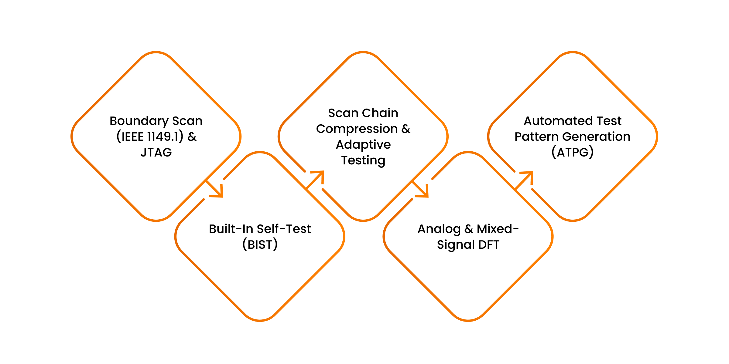
1. Boundary Scan (IEEE 1149.1) and JTAG
One of the most widespread and effective DFT techniques is Boundary Scan technology, also known as the Joint Test Action Group (JTAG) standard. It allows for testing the interconnections of ICs in a system without requiring physical access to each pin, which is especially useful for densely packed boards with limited space for probes.
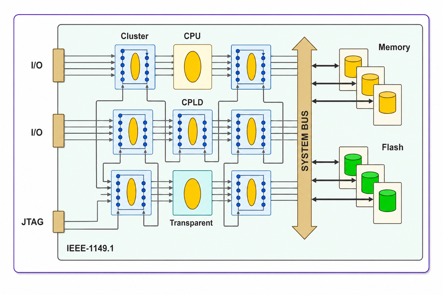
Source: https://www.blackhawk-dsp.com/products/jtag-software/boundary-scan
The diagram above depicts a system architecture that includes a cluster of CPUs, a CPLD, memory, flash storage, and input/output (I/O) interfaces. It features a JTAG (Joint Test Action Group) interface for testing and debugging purposes. The label “Transparent” likely refers to a component that facilitates seamless integration with other devices. Additionally, modern implementations support IEEE 1687 (IJTAG), enabling efficient access to embedded instruments and on-chip monitors in highly complex system-on-chip (SoC) designs.
Key benefits:
- Enables easier testing of board-level interconnects.
- Provides access to internal registers and memory for debugging purposes.
- Supports in-system programming, reducing the need for external equipment.
However, as systems become more complex, the boundary scan has evolved to meet the growing demands. Advanced versions include enhanced features for dealing with multi-chip modules and 3D ICs, allowing efficient testing of high-performance and heterogeneous systems.
2. Built-In Self-Test (BIST)
BIST is a technique where a circuit can test itself. Traditionally, external testing equipment was used to apply test patterns to an IC, but with BIST, these test patterns are generated and analyzed within the chip itself. BIST allows for at-speed testing and ensures that the circuit operates as expected under real-time conditions.
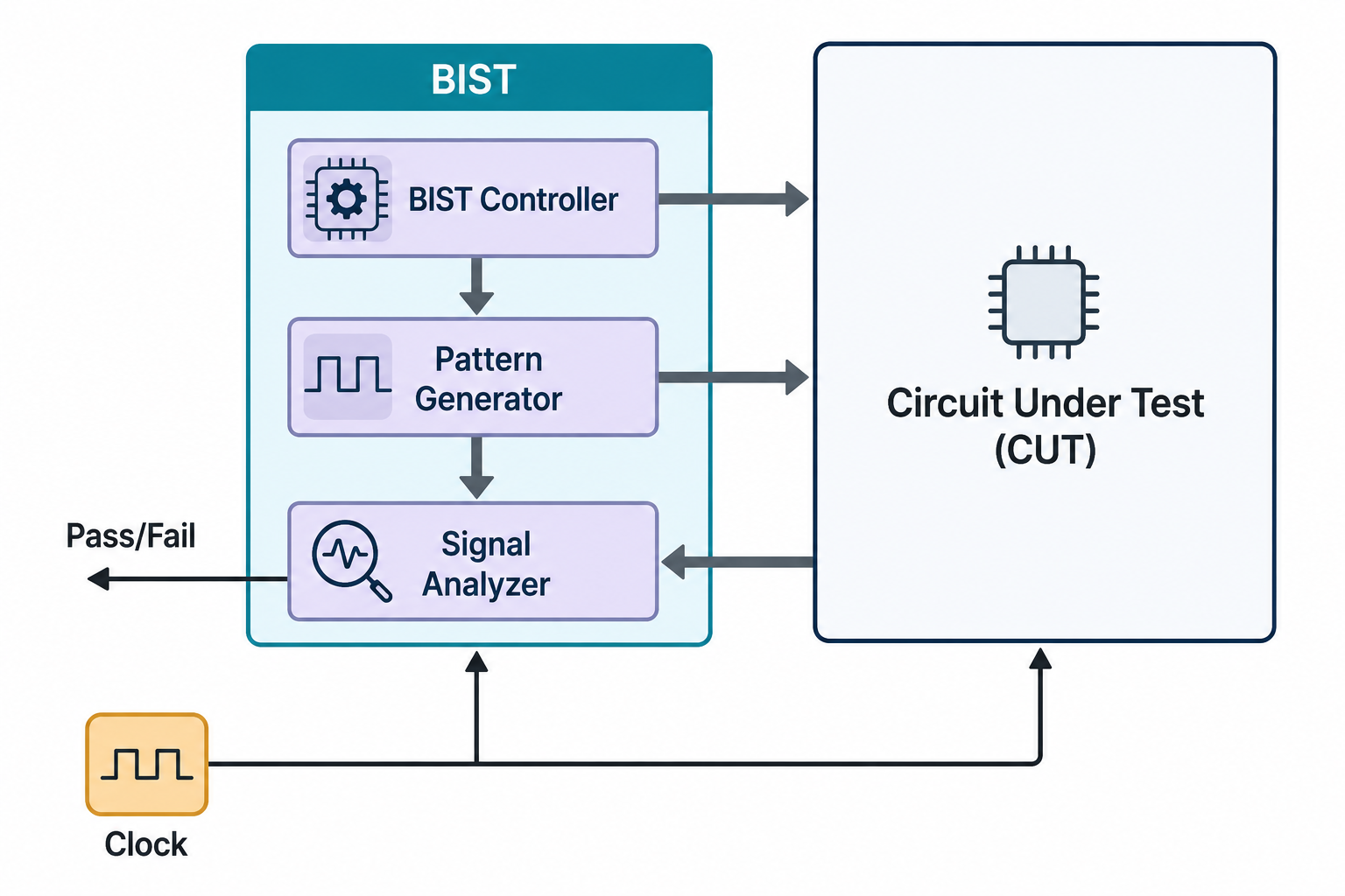
Source: https://www.sciencedirect.com/topics/computer-science/build-in-self-test
The above diagram shows a built-in self-test (BIST) system used to test integrated circuits. It consists of a controller, a pattern generator, a signal analyzer, and the circuit under test. There are several types of BIST techniques:
- Logic BIST (LBIST): Focuses on the internal logic of the chip.
- Memory BIST (MBIST): Specialized for testing memory components.
Advanced BIST techniques now support memory repair, at-speed testing, and AI-assisted test optimization to improve fault coverage while reducing overall test time.
3. Scan Chain Compression and Adaptive Testing
The concept of scan chain testing involves adding extra flip-flops to a design to make internal states observable. However, as the size of ICs has grown, so too has the length of these scan chains, leading to longer test times. Scan chain compression addresses this by reducing the amount of data needed for testing while maintaining fault coverage.
Another exciting development is the rise of adaptive testing, where real-time data from previous tests is analyzed to modify subsequent tests. This significantly reduces test time and improves efficiency.
Key Advantages:
- Faster test times.
- Reduced test data volume.
- Increased fault coverage, particularly for subtle defects
4. Analog and Mixed-Signal DFT
Testing analog and mixed-signal circuits presents unique challenges due to their continuous nature and sensitivity to noise. Traditional digital DFT techniques do not translate well into these domains. However, new Analog DFT methods have emerged, such as:
- On-chip analog stimulus generation: This provides controlled analog signals for testing circuits without the need for expensive external equipment.
- Sigma-delta modulation techniques: Used for high-resolution data conversion testing.
These innovations are key in industries such as automotive and healthcare, where mixed-signal devices are critical to sensors and communication systems. Mixed-signal DFT is also becoming increasingly important for RF, high-speed interface, and automotive safety applications requiring precise signal validation.
5. Automated Test Pattern Generation (ATPG)
ATPG has been a staple of DFT for years, but recent innovations have focused on improving its efficiency in detecting both random and systematic faults. Modern ATPG tools now incorporate machine learning and artificial intelligence to optimize test patterns based on real-time feedback. This ensures maximum fault coverage with minimal test time.
- Deterministic ATPG: Provides exact fault coverage with a comprehensive set of patterns.
- Random ATPG: Uses probabilistic patterns to detect hard-to-find defects.
By combining these techniques, advanced ATPG now offers a balance between cost and fault coverage. Test Engineering Services often leverage these advanced ATPG techniques to optimize testing processes. Today’s ATPG tools also support cell-aware testing, transition fault testing, and diagnosis-driven pattern generation for advanced technology nodes.
The Future of DFT: AI and Machine Learning Integration
The next frontier for DFT lies in the integration of artificial intelligence (AI) and machine learning (ML). By leveraging these technologies, it is possible to analyze vast amounts of test data, detect patterns, and predict failures more accurately than ever before. AI-driven DFT techniques will allow for more efficient test scheduling, smarter diagnostics, and adaptive testing strategies that evolve with each new generation of ICs.
Emerging technologies such as chiplet-based systems, heterogeneous integration, and 3D-ICs are also driving the development of next-generation DFT solutions capable of testing increasingly complex semiconductor architectures.
The Future of Test Engineering: How Automation is Changing the Game
Let’s Conclude
As ICs continue to advance in complexity and performance, so too must the techniques used to test them. Advanced DFT techniques such as boundary scan, BIST, scan chain compression, and ATPG are pivotal in ensuring reliable, cost-effective testing in modern IC design. The integration of AI and machine learning promises to drive further innovation in this field, helping streamline testing processes and improve fault detection accuracy.
As semiconductor technologies continue to evolve toward AI computing, advanced packaging, and smaller process nodes, intelligent DFT methodologies will remain essential for ensuring product quality, reliability, and manufacturing efficiency.
Therefore, by investing in these innovations, the semiconductor industry can continue to push the boundaries of technology while ensuring that quality and reliability remain at the forefront. Semiconductor test engineers and Test Engineering Services play a crucial role in this ongoing evolution.
Frequently Asked Questions
1. What is Design-for-Test (DFT) in semiconductor engineering?
Design-for-Test (DFT) integrates test features into ICs, improving fault detection, manufacturing quality, test coverage, and production efficiency.
2. Why is DFT important in chip design?
DFT simplifies IC testing, reduces manufacturing costs, improves yield, shortens test time, and ensures reliable semiconductor performance.
3. What are the most common DFT techniques used in semiconductor design?
Common DFT techniques include scan chains, Boundary Scan (JTAG), Built-In Self-Test (BIST), Memory BIST, and Automated Test Pattern Generation (ATPG).
4. What does a Design-for-Test engineer do?
A DFT engineer develops test architectures, implements scan logic, verifies testability, and improves fault coverage before semiconductor manufacturing.
5. How do DFT services improve semiconductor testing?
DFT services optimize chip testability through advanced architectures, automated test patterns, scan insertion, and fault analysis, reducing production risks and costs.