

Nowadays, the semiconductor industry is under constant pressure. They have to deliver more powerful, efficient, and reliable chips within increasingly compressed development cycles. However, the traditional approach that was used for semiconductor testing often occurred late in the development cycle, could be costly and inefficient for the current conditions. Therefore, companies now use the Shift Left Testing methodology that flips the script by moving testing earlier in the process.
Shift Left Testing process not helps in increasing quality, delivery speed, and in optimizing the budget.
What Is Shift Left Testing?
Shift left testing is a proactive engineering approach in the semiconductor and Electronic Design Automation (EDA) that brings testing, verification, and validation into the early stages of IC design and development. Instead of relying on post-silicon prototypes or late-stage lab testing to uncover issues, engineering teams use advanced simulation, emulation, and verification tools to detect and resolve potential design challenges much earlier. By identifying defects before they propagate through the development cycle, organizations can reduce costly redesigns, shorten development timelines, and deliver higher-quality silicon with greater confidence.
What Does Shift Left Testing Mean In Semiconductor Engineering?
Often, shift left testing is misunderstood as simply testing earlier, but in reality it represents a broader engineering philosophy. It helps in checking the quality throughout the product lifecycle.
Semiconductor development involves test engineering services across multiple stages, including:
- Architecture planning
- RTL design and verification
- Design-for-Test (DFT) implementation
- Functional simulation
- Emulation and FPGA prototyping
- Test program development
- Continuous validation
Engineering teams can identify functional, structural, and manufacturing risks during the design process. They do not have to wait for silicon availability to begin validation. This early collaboration between design, DFT, validation, and manufacturing teams helps eliminate defects before they become expensive engineering problems.
How Early Engineering Accelerates Time To Market?
Shift-left engineering accelerates semiconductor development by implementing testing, verification, and collaboration early in the design lifecycle.
1. Early DFT Planning
Design-for-Test (DFT) is no longer limited to the final stages of chip development. Integration of DFT during the architecture and RTL phases allows engineering teams to build testability into the design from the outset. Early planning helps optimize scan insertion, improve fault coverage, and ensure manufacturing readiness before implementation begins. This reduces costly redesign cycles while enhancing test efficiency and product quality throughout the semiconductor lifecycle.
2. Continuous Verification Throughout Development
Semiconductor development now relies on continuous verification rather than waiting for the final validation stage. Throughout the design cycle, engineering teams use a combination of:
- RTL simulation
- Formal verification
- Functional coverage analysis
- Emulation
- FPGA prototyping
By uncovering functional issues during RTL development, teams can resolve defects when they are faster and more cost-effective to fix. Addressing these challenges early helps avoid expensive silicon respins, minimizes project risks, and keeps development schedules on track.
Ensuring First-Pass Success with VLSI Verification Strategies
3. Parallel Test Program Development
In traditional workflows, Automated Test Equipment (ATE testing) programs are typically developed only after the first silicon becomes available. Shift Left Engineering changes this approach by allowing test program development for DFT coverage to progress in parallel with chip design.
Developing test programs and validation alongside the design process enables faster silicon bring-up, shortens production qualification cycles, and improves overall manufacturing readiness. As a result, organizations can accelerate product validation and move from first silicon to volume production more efficiently.
4. Cross-Functional Collaboration
Delivering complex semiconductor products requires close collaboration across multiple engineering teams. Shift Left Engineering encourages cross-functional engagement from the earliest design stages, bringing together:
- Design engineers
- Verification teams
- DFT specialists
- Validation engineers
- Manufacturing teams
- Test engineers
This collaborative approach helps in identifying and resolving issues before they become costly bottlenecks. By breaking down silos and enabling continuous communication throughout development, teams can make faster decisions, reduce engineering rework, and bring high-quality products to market sooner.
Business Benefits Of Shifting Test Left
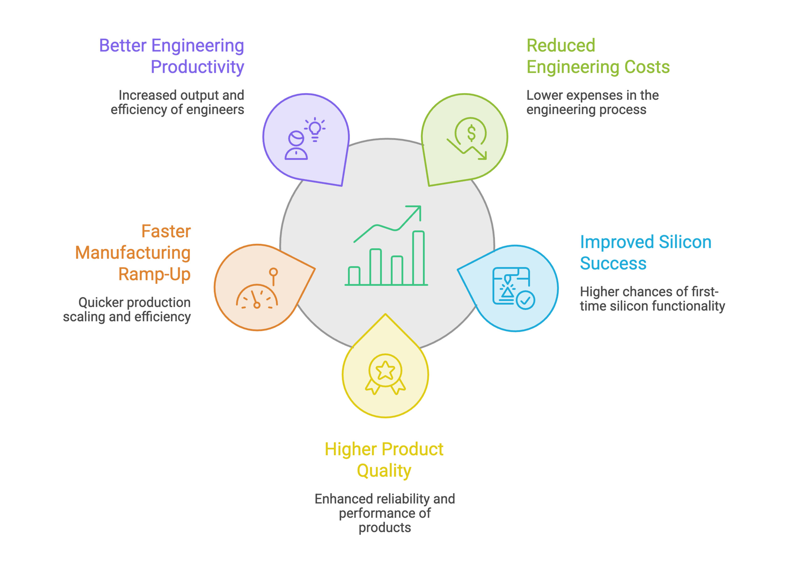
Faster product releases are a major advantage in today’s world, and shift left delivers value across the entire semiconductor lifecycle.
- Reduced Engineering Costs: It reduces the cost by identifying defects earlier. Organizations minimize expensive redesigns and reduce the overall development cost.
- Improved First-Pass Silicon Success: Late-stage design issues frequently result in silicon respins among the costliest setbacks in semiconductor development.
- Higher Product Quality: Continuous testing throughout development improves functional correctness, manufacturing readiness, and long-term product reliability.
- Faster Manufacturing Ramp-Up: Products that undergo pre-silicon validation typically require fewer production adjustments. Manufacturing teams receive better-tested designs, enabling smoother production ramp-up and faster customer deliveries.
- Better Engineering Productivity: Instead of spending months debugging preventable issues, engineering teams can focus on innovation, optimization, and new product development.
Industry Trends Driving Shift Left Engineering
As semiconductor designs grow more complex, Shift Left Engineering is becoming a strategic approach for improving development efficiency, product quality, and time-to-market. Several industry trends are accelerating its adoption across the semiconductor lifecycle.
AI-Assisted Verification
Artificial intelligence is transforming semiconductor testing services by helping engineering teams identify design anomalies, prioritize high-risk test scenarios, and automate repetitive verification tasks. By uncovering potential issues earlier in the design cycle, AI-driven verification improves coverage, shortens debug time, and supports the development of increasingly complex SoCs and AI accelerators.
Earlier Design-for-Test (DFT) Integration
Design-for-Test is now being incorporated much earlier in the development process, with scan planning, fault analysis, and test architecture decisions beginning during the RTL phase. This early integration enhances testability, simplifies downstream implementation, and improves fault coverage while reducing engineering rework.
Silicon-To-System Validation
Semiconductor validation is expanding beyond individual chips to encompass complete systems. By combining pre-silicon verification, post-silicon validation, embedded software testing, and manufacturing test into a continuous workflow, organizations can improve product reliability, streamline system-level validation, and accelerate the path from silicon to production.
How Tessolve Enables Shift Left Engineering?
By tapping the large pool of experienced design and test engineers, Tessolve enables Shift-Left testing by integrating, verification, Design-for-Test (DFT), emulation, and validation early in the semiconductor development lifecycle. Through advanced pre-silicon testing, virtual prototyping, and automated test engineering, we help identify design issues before fabrication, reducing respins, accelerating silicon bring-up, and improving product quality. Our end-to-end engineering expertise supports faster time-to-market for AI, automotive, and high-performance semiconductor products.
Frequently Asked Questions (FAQs)
1. What does Shift Left mean in semiconductor testing?
Shift Left integrates semiconductor testability and test engineering early, identifying defects sooner to reduce development time and improve product quality.
2. How does Shift Left test engineering accelerate time-to-market?
Shift Left test engineering helps to identify design and testability issues early, reducing respins, validation cycles, and overall semiconductor product development time.
3. How does Shift Left improve SoC and IC testing?
Adoption of this methodology results in early verification, improved fault coverage, simplified debugging, and increased likelihood of first-pass silicon success.
Source Links
- https://www.cadence.com/en_US/home/explore/what-is-shift-left-testing.html
- https://semiengineering.com/shift-left-strategy-for-semiconductor-production-testing/
- https://www.relevancelab.com/post/shift-left-testing-basics
- https://www.tessolve.com/blogs/from-silicon-to-system-the-new-era-of-end-to-end-test-engineering/
- https://totalshiftleft.com/blog/shift-left-testing-complete-guide
- https://buildpiper.io/blogs/understanding-the-concept-of-shift-left/