In the ever-evolving landscape of technology, semiconductor testing stands at the forefront, driving innovation and shaping the future of electronic devices. With the rise of AI processors, chiplet-based architectures, advanced packaging, and high-performance computing, semiconductor testing has become more critical than ever. Tessolve, a leading semiconductor engineering company, continues to drive innovation in semiconductor engineering solutions. In this blog, we delve into the latest advancements reshaping modern semiconductor testing.
Automated Test Equipment (ATE) Revolution
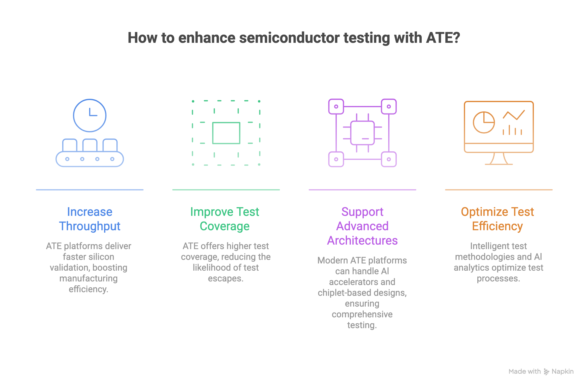
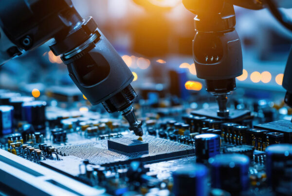
Automated Test Equipment (ATE) has evolved significantly to address the demands of advanced semiconductor devices. Modern ATE platforms support AI accelerators, chiplet-based architectures, advanced packaging, and high-speed interfaces while delivering higher test coverage, improved throughput, and faster silicon validation. Intelligent test methodologies, AI-driven test analytics, and predictive yield learning further help optimize test efficiency, reduce test escapes, and improve manufacturing yield.
Advanced Probe Technologies
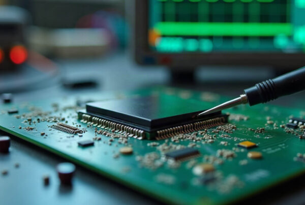
Precision is paramount in semiconductor testing, and Tessolve is at the forefront with its cutting-edge probe technologies. Micro-electro-mechanical systems (MEMS) based probes have gained prominence, offering superior contact accuracy and reduced signal interference. Modern probe technologies also support wafer-level testing and fine-pitch devices used in advanced process nodes. These probes are instrumental in testing high-density integrated circuits, enabling faster data transfer rates, less interconnect losses, and thus ensuring the functionality of Device Under Test (DUT).
3D IC Testing
Three-dimensional Integrated Circuits (3D ICs), chiplet-based architectures, UCIe-enabled multi-die systems, and advanced packaging technologies have become a standard in modern electronics. However, testing these densely packed layers of circuits poses significant challenges. Tessolve has pioneered non-destructive testing techniques using advanced X-ray CT, thermal imaging, and other inspection technologies. These methods allow for comprehensive analysis of complex multi-die devices without damaging the delicate layers, ensuring the production of flawless chips.
System-in-Package (SiP) Testing
System-in-Package (SiP) technology continues to gain traction by enabling heterogeneous integration of processors, memory, RF components, and AI accelerators within compact packages. Tessolve has developed innovative testing solutions for SiP modules, ensuring seamless integration of diverse components like microprocessors, memory, and sensors. This integrated approach streamlines the testing process, reducing time-to-market for electronic devices.
High-Frequency Testing
With the rapid growth of 5G, Wi-Fi 7, automotive radar, and emerging 6G research, high-frequency testing has become imperative. Tessolve has introduced state-of-the-art radio-frequency (RF) testing equipment capable of handling ultra-high frequencies. This technology is pivotal in ensuring the reliability of wireless communication devices, paving the way for the next generation of connectivity.
Reliability Testing and Failure Analysis
Reliability testing is critical to guarantee the longevity of semiconductor devices. Tessolve employs accelerated stress testing methods, such as the Highly Accelerated Stress Test (HAST) and Temperature-Humidity-Bias (THB), to simulate extreme environmental conditions. Additionally, advanced failure analysis techniques, including Electron Beam Testing, Lock-in Thermography, and Atomic Force Microscopy, are employed to identify and rectify defects at the microscopic level, ensuring robust and durable semiconductor products.
Security Testing
As cybersecurity remains a significant concern, Tessolve has made substantial investments to improve its security testing protocols. The company employs advanced techniques like Side-Channel Analysis and Fault Injection Attacks, along with hardware security validation for secure boot and a hardware root of trust. These methods are used to identify vulnerabilities in semiconductor devices. By enhancing chip security against potential breaches, Tessolve plays a crucial role in safeguarding sensitive data within electronic systems.
Environmental Sustainability
In the wake of environmental consciousness, Tessolve has embraced eco-friendly testing practices. Energy-efficient testing equipment and AI-assisted optimized testing algorithms reduce power consumption significantly. Additionally, the company has implemented responsible waste management processes, minimizing the environmental impact of semiconductor testing operations.
Optimal Approaches for Designing High-Speed Printed Circuit Boards
Wafer-Level Testing
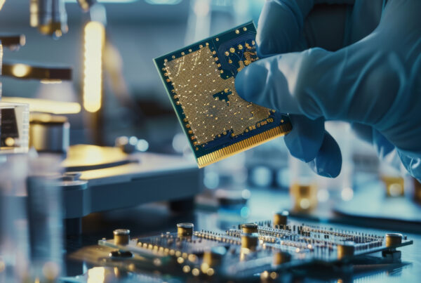
As semiconductor devices continue to shrink and advanced packaging technologies become mainstream, wafer-level testing has become increasingly important. Modern semiconductor testing emphasizes Known Good Die (KGD) validation before packaging, helping reduce manufacturing costs and improve final product yield. Advanced probe cards with fine-pitch probing capabilities enable accurate electrical testing of AI processors, HBM, chiplets, and other high-density devices directly at the wafer stage. This approach identifies defects earlier, shortens production cycles, and improves the reliability of advanced semiconductor produc
Silicon Photonics & High-Speed Interconnect Testing
The rapid growth of AI data centers, cloud computing, and high-performance computing has accelerated the adoption of silicon photonics and ultra-high-speed interconnects. Modern semiconductor devices increasingly rely on 112G/224G SerDes interfaces to enable high-bandwidth, low-latency communication between processors, memory, and networking equipment. Testing these high-speed interfaces requires advanced RF measurement techniques, precise signal integrity analysis, and specialized validation methodologies to ensure reliable performance in next-generation computing and communication systems.
Wrapping Up
As we navigate the intricate world of semiconductor testing in 2023, Tessolve stands as a beacon of innovation and technical excellence. By pushing the boundaries of what is possible, Tessolve continues to drive the industry forward, ensuring the production of reliable, high-performance electronic devices that shape our interconnected world. With a relentless pursuit of excellence and a commitment to technological advancement in semiconductor engineering, Tessolve remains at the forefront of the semiconductor testing revolution, shaping the future one chip at a time.
Frequently Asked Questions
1. What are the latest advancements in semiconductor technology?
The latest advancements in semiconductor technology include AI processors, chiplet architectures, advanced packaging, silicon photonics, and high-speed interconnect testing.
2. What is advanced semiconductor testing, and why is it important?
Advanced semiconductor testing validates complex chips using AI-driven analytics, wafer-level testing, and high-speed electrical validation to improve reliability and yield.
3. How can semiconductor test solutions help reduce time-to-market for new semiconductor products?
Modern semiconductor test solutions accelerate validation, improve defect detection, reduce rework, and shorten production cycles for faster product launches.
4. What test equipment is used for System-in-Package (SiP) semiconductor testing?
Test equipment for System-in-Package (SiP) includes advanced ATE platforms, probe cards, RF measurement systems, and electrical validation tools.
5. What are the latest semiconductor testing equipment updates?
Recent semiconductor testing equipment updates focus on AI-assisted automation, wafer-level testing, high-speed I/O validation, and advanced failure analysis technologies.