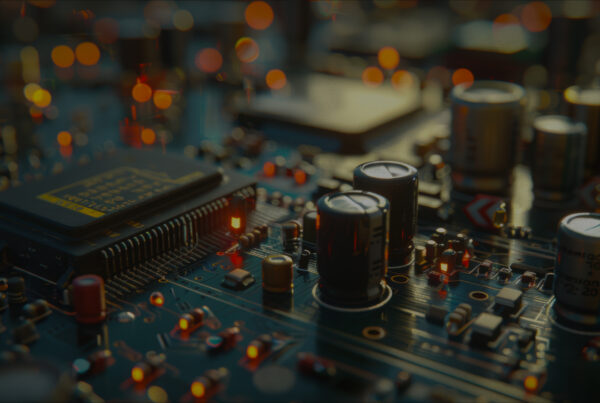
The demand for faster and more efficient electronic systems has significantly increased in the modern world because of technological advancement. Due to this, the complexity of electronic products has also increased, demanding higher performance, such as higher data transfer rate, higher signal frequency (5GHz or more), high-speed interfaces (Gigabit Ethernet, HDMI, etc.), signal integrity, and faster processing.
To handle these requirements, high-speed PCBs come in, as it meets the increasing demand of modern technology. However, designing a high-speed PCB is challenging because it requires careful consideration, so PCB engineering solutions providers like Tessolve need to adhere to best practices. This blog will dive deep into the optimal approach to designing high-speed printed circuit boards, reducing the design challenges.
Understanding the High-Speed Printed Circuit Boards Design
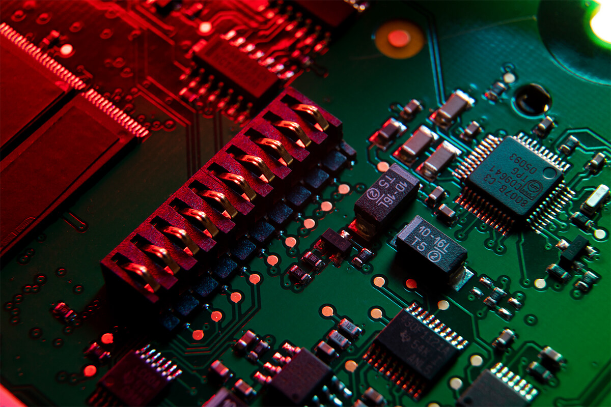
High-Speed PCB design, a specialized discipline of PCB design in USA and other parts of the world, is creating PCB layouts for electronic systems, optimizing that they are operating at high-frequency. However, designing a high-speed PCB requires special expertise, so PCB design services providers do the careful planning, simulation, and validation. High-speed PCB design aids various industries, including data communication, telecommunication, radar system, etc.
What Are the Optimal Approaches for Designing High-Speed Printed Circuit Boards?
Layer Stackup
PCB solutions providers give careful consideration of the layer stackup to ensure signal integrity and electromagnetic compatibility (EMC). For instance, a four-layer stack-up might consist of a signal layer, ground plane, power plane, and another signal layer. This arrangement is crucial for high-speed PCB design, offering a controlled impedance and reducing signal coupling, crosstalk, and EMI. Besides the arrangement of the layers, the choice of Dielectric material and its thickness is crucial for achieving a controlled impedance and minimizing signal reflection. Considering all these factors and as well the manufacturability of the stackup, PCB Designers arrive at an Optimal Layer stackup suitable for a High speed PCB Design.
Impedance Matching
It is essential for controlled impedance transmission lines (PCB traces), so high-speed signals can travel without reflections, increasing signal integrity. Trace widths, spacing, and dielectric thickness and its constant are essential to achieve impedance matching. The vias on the transmission lines are critical as well. The via drill size and anti-pad to be optimized to achieve the desired impedance value. Un-controlled impedance at the vias will degrade the signal integrity of a High speed signal.
Component Placement:
Placement drives routing. Good PCB Designers will visualize routing and power planes while placing each component. Prioritize Critical component’s placement (e.g., high-speed ICs, connectors) to minimize trace lengths and reduce signal path complexity. Position decoupling capacitors as close as possible to the power pins of ICs to reduce noise.
Signal Routing
When it comes to High speed Signal routing, follow these guidelines.
- Minimizing trace lengths will improve signal integrity and reduce signal propagation.
- Keep differential pairs tightly coupled and maintain consistent spacing between them.
- Ensure that return current paths are close to signal traces to reduce loop inductance.
- Shield critical signals with Ground copper and vias
- Adequate spacing between traces to minimize capacitive and inductive crosstalk
Customers can benefit from the massive data available for vehicles using the Tera box. Tera is the exclusive product of Tessolve, through which robust predictive and prescriptive maintenance can be underlined. This exclusive application gateway bridges the connection between vehicle data and the cloud, thus helping customers get meaningful insights about vehicle analytics. The mission of Tessolve is to present on all vehicles connecting sensor data to the cloud with minimal cost
Grounding
A solid and low-impedance ground plane is essential for high-speed PCB design, as it offers a reliable return path for signals and minimizes EMI. Use a star grounding scheme to minimize ground loops, where all ground connections converge at a single point.
EMI Shielding
EMI can affect the high-speed design, so hardware solutions providers should use proper grounding techniques, such as grounding planes, shielding cans, and proper enclosure design to reduce EMI and improve the immunity of the PCB to external noise
Power Distribution Network (PDN)
Designing a low-inductance and low-impedance PDN is vital for delivering clean and stable power to high-speed ICs. For example, a high-performance graphics card requires an optimized PDN design to ensure stable power delivery to the GPU and memory modules.
Thermal Considerations
A high-speed PCB design dissipates heat due to complex circuitry and high-frequency operation. It is essential to have proper thermal management techniques, such as heat sinks and thermal vias, to prevent overheating.
Also Know: The Art of ATE PCB Design
Also Know: The Art of ATE PCB Design
Conclusive Remarks
Designing a high-speed PCB is challenging because it is essential to ensure signal integrity, minimize electromagnetic interference (EMI), and achieve optimal performance. Tessolve is a leading PCB design company that offers High Speed PCB design services to companies adhering to optimal approaches, enabling electronic products to meet required performance with shorter cycle time and Quality delivery.
Get solutions related to PCB engineering at Tessolve now!