Printed Circuit Board (PCB) design is both a science and an art, requiring a deep understanding of electrical engineering principles, materials science, and manufacturing processes. It becomes significantly more complex when designing an Automated Test Equipment (ATE) PCB, which is widely used for high-speed functional, parametric, and reliability testing of semiconductor ICs, such as:
- Microprocessors
- Memory chips (DDR, HBM)
- System-on-Chip (SoC)
- Graphics Processing Units (GPUs)
- Analog and Mixed-Signal ICs
- Power Management ICs
The art of ATE PCB design involves balancing several competing factors to create a functional and efficient hardware to test the Device Under Test (DUT). So, in this blog, we will go through some of the factors you must consider while designing an ATE PCB.
Signal Integrity
Signal Integrity refers to the ability of electrical signals to maintain their quality and accuracy as they travel through the PCB. As ATE PCBs are meant to test Semiconductor chips, the quality of the PCB is paramount as it affects the accuracy and reliability of the test results. Factors like Trace impedance mismatch, Signal reflections, and Noise can affect the Signal Integrity. Best practices such as balanced PCB stack-up, tightly controlled impedance lines, good termination, and reducing via stubs can help to maintain the Signal Integrity.
Power Integrity
Power Integrity refers to the stability and reliability of a PCB’s power delivery system. To test today’s low-voltage and power-sensitive semiconductors, ATE PCBs need to be designed with a good Power Distribution Network (PDN). It plays a crucial role in ensuring stable voltage levels, reducing power noise and losses, and improving overall power efficiency. Solid power planes, optimized PCB stack-up, and De-coupling capacitor’s value and placement are crucial in ensuring good PDN design in ATE PCBs.
Mechanical Constraints
ATE PCBs connect to various equipment such as test heads, handlers, and probers for high-volume automated IC testing. Each type of equipment has specific mechanical requirements that must be considered during the ATE PCB design process. When the device under test (DUT) is an RF device, it is essential to position the cables and their connectors on the PCB as close to the DUT as possible to facilitate connections with RF test instruments. Adhering to these mechanical constraints helps prevent the need for PCB re-spins. ATE PCB designers collaborate closely with mechanical engineers to define placement constraints and validate the completed design for any violations.
Multi-Layered PCB
The complexity and electrical requirements of the ATE PCBs call for a multi-layered structure. The high routing density and the need for dedicated layers for Power, Ground, and Signals increase the layer count to a Max of 80 layers in the case of a complex ATE PCB. Multi-layer PCBs have a tendency to warp when it undergoes the reflow soldering process. The PCB is made up of different types of materials: resin, glass fibers, and copper. Each material has its own thermal properties, and when the PCB undergoes a thermal cycle, the materials expand at a different rate, causing the PCB to warp. A balanced Multi-layer PCB helps to control the warpage within limits.
Advanced Via Technology
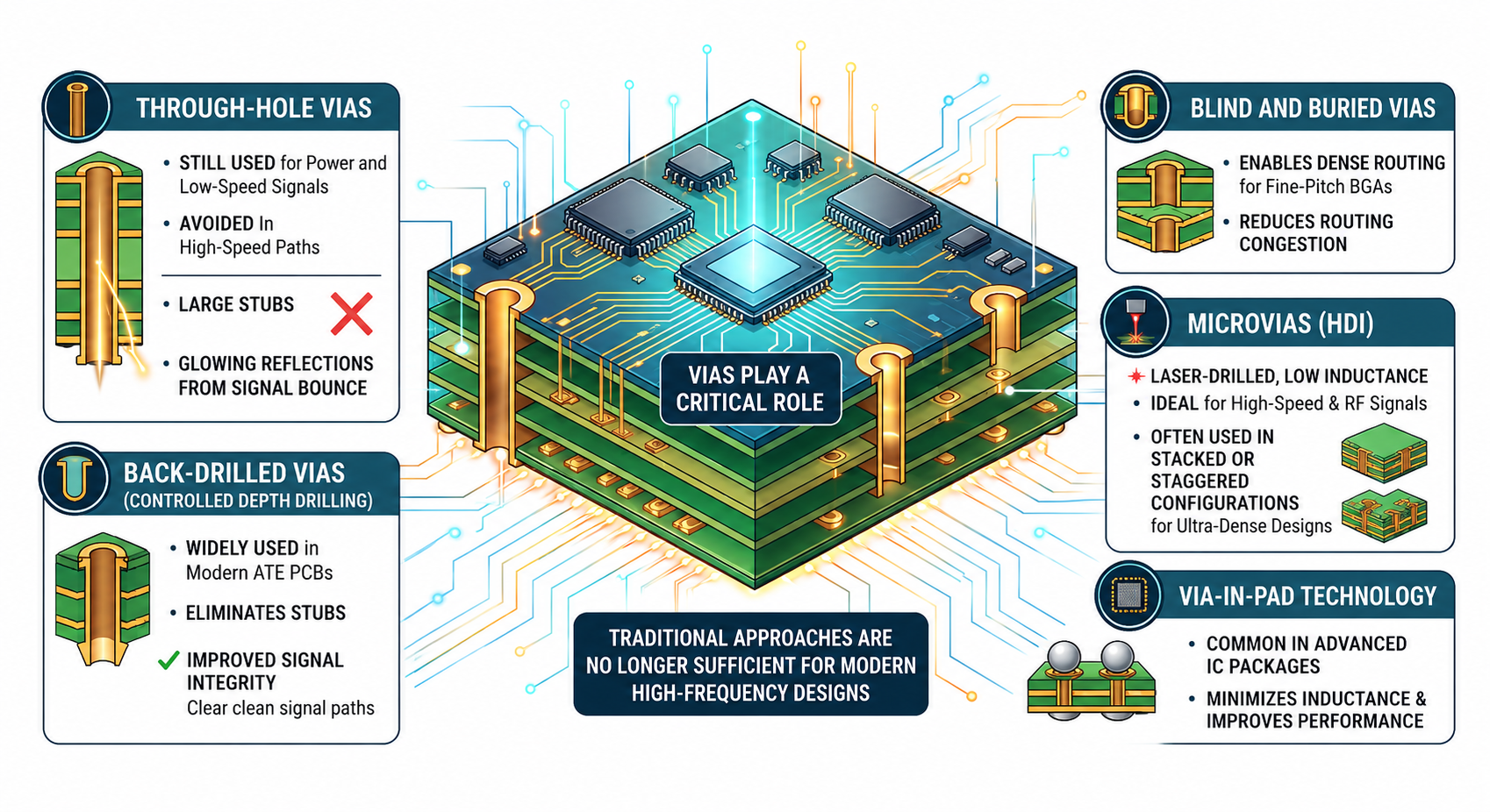
Vias play a critical role in high-speed ATE PCB performance. Traditional via approaches are no longer sufficient for modern high-frequency designs.
Updated via strategies include:
- Through-hole vias: Still used for power and low-speed signals, but avoided in high-speed paths due to large stubs
- Back-drilled vias (Controlled Depth Drilling): Widely used in modern ATE PCBs to eliminate stubs and improve signal integrity
- Blind and Buried vias: Enable dense routing for fine-pitch BGAs and reduce routing congestion
- Microvias (HDI):Laser-drilled, low inductance, ideal for high-speed and RF signals Often used in stacked or staggered configurations for ultra-dense designs
- Via-in-pad technology: Common in advanced IC packages for minimizing inductance and improving performance
Choosing the right via strategy directly impacts signal performance, manufacturability, and cost.
Thermal Management (New Critical Consideration)
Modern ATE PCBs must handle high power densities due to advanced IC testing, especially for GPUs, AI chips, and high-performance SoCs.
Key strategies include:
- Thermal vias and heat spreading planes
- Use of high thermal conductivity materials
- Active cooling interfaces in test setups
- Thermal simulation during the design phase
Proper thermal management ensures consistent test conditions and prevents measurement drift.
Conclusion
Designing ATE PCBs today goes far beyond traditional PCB practices. It requires expertise in high-speed design, advanced materials, signal and power integrity, and system-level integration.
Tessolve PCB team brings extensive experience in high-complexity ATE PCB design, supporting advanced semiconductor testing requirements across global clients. Their designs have been recognized with the Siemens Xcelerator Technology Innovation Awards (2020 & 2022), showcasing excellence in innovation and engineering precision.
If you are looking to design next-generation ATE PCBs for high-speed and high-reliability applications, Tessolve offers the expertise and proven track record to deliver exceptional results.
FAQs
1. What is an ATE PCB, and why is it important?
An ATE PCB is used to test semiconductor ICs, ensuring accurate performance validation, reliability, and quality during production.
2. What are the key challenges in ATE PCB design?
Major challenges include maintaining signal integrity, ensuring power stability, handling high-speed signals, and meeting mechanical constraints.
3. How does signal integrity impact ATE PCB performance?
Poor signal integrity causes distortion, reflections, and noise, leading to inaccurate test results and unreliable semiconductor validation.
4. Why are multilayer PCBs used in ATE applications?
Multilayer PCBs support dense routing, separate power and signal layers, and enable high-speed performance in complex testing environments.
5. What role does Via technology play in ATE PCB design?
Via selection affects signal quality, routing density, and manufacturability, especially in high-speed and high-frequency PCB designs.