In the ever-evolving landscape of technology, semiconductor testing stands at the forefront, driving innovation and shaping the future of electronic devices. As we step into 2023, Tessolve, a pioneer semiconductor design company in semiconductor engineering solutions, continues to lead the way in revolutionizing the industry. In this blog, we delve deep into the technical advancements that are reshaping semiconductor testing in 2023.
Automated Test Equipment (ATE) Revolution
High-Speed PCB design, a specialized discipline of PCB design in USA and other parts of the world, is creating PCB layouts for electronic systems, optimizing that they are operating at high-frequency. However, designing a high-speed PCB requires special expertise, so PCB design services providers do the careful planning, simulation, and validation. High-speed PCB design aids various industries, including data communication, telecommunication, radar system, etc.
Advanced Probe Technologies
Precision is paramount in semiconductor testing, and Tessolve is at the forefront with its cutting-edge probe technologies. Micro-electro-mechanical systems (MEMS) based probes have gained prominence, offering superior contact accuracy and reduced signal interference. These probes are instrumental in testing high-density integrated circuits, enabling faster data transfer rates, less interconnect losses and thus ensuring the functionality of Device Under Test (DUT).
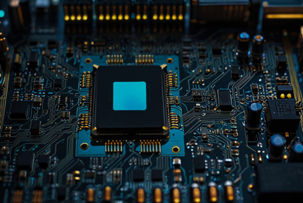
3D IC Testing
Three-dimensional Integrated Circuits (3D ICs) have become a standard in modern electronics. However, semiconductor systems integrator testing these densely packed layers of circuits poses significant challenges. Tessolve has pioneered non-destructive testing techniques using advanced X-ray and thermal imaging. These methods allow for comprehensive analysis of 3D ICs without damaging the delicate layers, ensuring the production of flawless chips.
System-in-Package (SiP) Testing
System-in-Package technology has gained traction in the semiconductor industry due to its compact design and enhanced performance. Tessolve has developed innovative testing solutions for SiP modules, ensuring seamless integration of diverse components like microprocessors, memory, and sensors. This integrated approach streamlines the testing process, reducing time-to-market for electronic devices.
High-Frequency Testing
With the advent of 5G technology and beyond, high-frequency testing has become imperative. Tessolve has introduced state-of-the-art radio-frequency (RF) testing equipment capable of handling ultra-high frequencies. This technology is pivotal in ensuring the reliability of wireless communication devices, paving the way for the next generation of connectivity.
Reliability Testing and Failure Analysis
Reliability testing is critical to guarantee the longevity of semiconductor devices. Tessolve employs accelerated stress testing methods, such as the Highly Accelerated Stress Test (HAST) and Temperature Humidity Bias (THB), to simulate extreme environmental conditions. Additionally, advanced failure analysis techniques, including Electron Beam Testing and Atomic Force Microscopy, are employed to identify and rectify defects at the microscopic level, ensuring robust and durable semiconductor products.
Security Testing
With cybersecurity becoming a paramount concern, Tessolve has invested heavily in enhancing security testing protocols. Advanced techniques such as Side-Channel Analysis and Fault Injection Attacks are employed to identify vulnerabilities in semiconductor devices. By ensuring the security of chips against potential breaches, Tessolve contributes significantly to protecting sensitive data in electronic systems.
Environmental Sustainability
In the wake of environmental consciousness, Tessolve has embraced eco-friendly testing practices. Energy-efficient testing equipment and optimized testing algorithms reduce power consumption significantly. Additionally, the company has implemented responsible waste management processes, minimizing the environmental impact of semiconductor testing operations.
Also Know: Optimal Approaches for Designing High-Speed Printed Circuit Boards
Wrapping Up
As we navigate the intricate world of semiconductor testing in 2023, Tessolve stands as a beacon of innovation and technical excellence. By pushing the boundaries of what is possible, Tessolve continues to drive the industry forward, ensuring the production of reliable, high-performance electronic devices that shape our interconnected world. With a relentless pursuit of excellence and a commitment to technological advancement in semiconductor engineering, Tessolve remains at the forefront of the semiconductor testing revolution, shaping the future one chip at a time.