

Every electronic device we use today, from smartphones and medical monitoring systems to industrial machines and automotive control units, depends on a well-designed Printed Circuit Board (PCB). The PCB acts as the backbone of modern electronics, enabling components to communicate, distributing power efficiently, and ensuring stable system operation.
Reliability is especially important in industries such as automotive electronics, consumer devices, medical equipment, industrial automation, and aerospace hardware. This same level of reliability is now equally crucial for AI edge devices, robotics, and connected IoT systems, where uninterrupted operation and low failure rates are essential. In these sectors, even minor design flaws can lead to performance issues or system failures.
Designing a PCB goes far beyond connecting components. Engineers must consider signal integrity, thermal behavior, power delivery, power integrity (PI), electromagnetic compatibility (EMC), and manufacturability. This is where a professional PCB design service becomes essential in guiding hardware from concept to production while maintaining reliability and performance.
The PCB Development Journey: From Concept to Production
Designing reliable hardware is not a simple, one-step task. It requires a structured engineering process that progresses through several stages. This process begins with defining system requirements and culminates in large-scale manufacturing. Each stage is crucial to ensuring that the final product performs reliably under real-world conditions.
From selecting components and designing schematics to validating prototypes and preparing the board for manufacturing, every phase contributes to building a stable and scalable PCB solution. Modern development workflows also emphasize early validation, cross-functional collaboration, and Design for Manufacturability (DFM) to reduce redesign cycles. The following stages outline how professional engineering teams transform an idea into production-ready hardware using a systematic PCB design approach.
Stage 1: Turning an Idea into a Hardware Concept
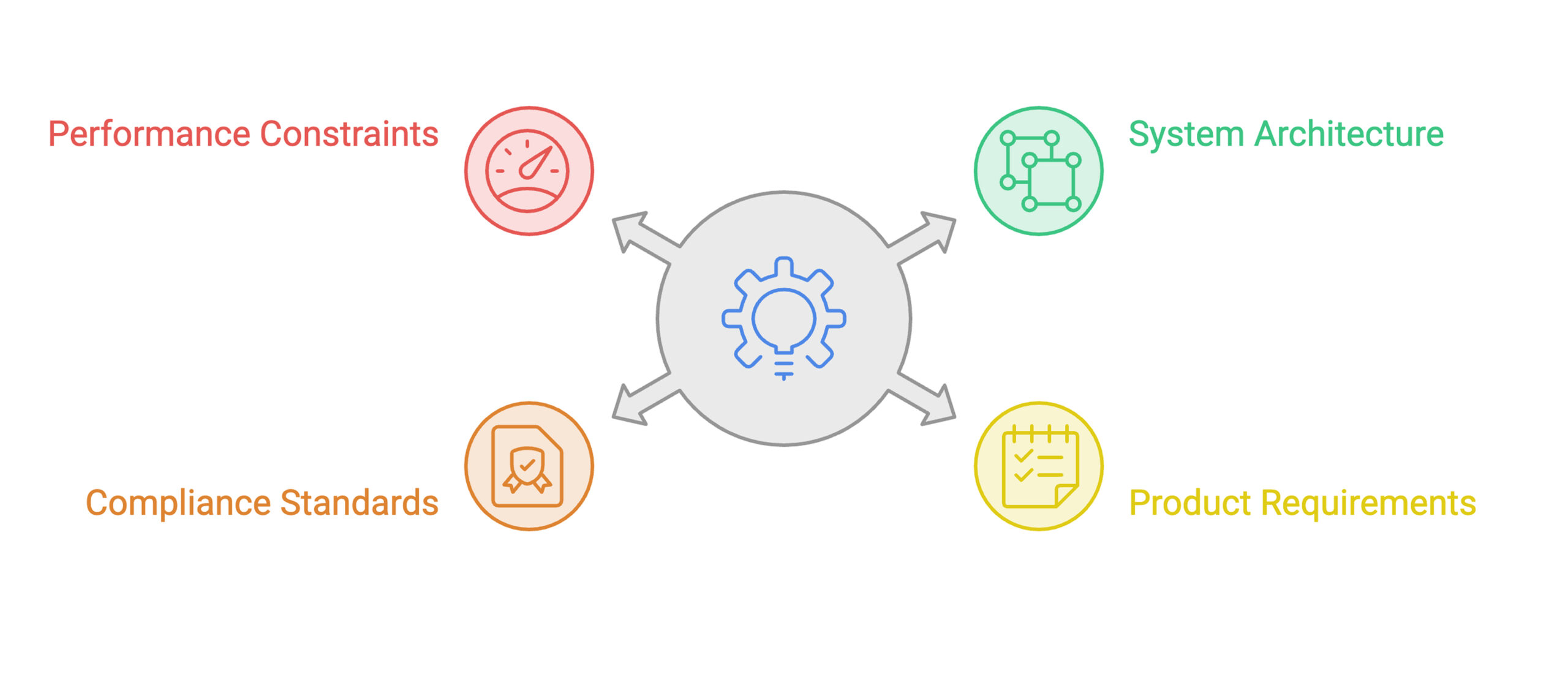
Successful hardware products start with a well-defined concept and clearly structured system requirements. Before engineers begin designing circuits or planning board layouts, they need to understand the device’s objectives and how it will function in real-world environments. This initial planning stage is crucial in shaping the overall approach to PCB engineering.
Product Requirements
The first step is defining the functional goals of the device. Engineers must determine what the system is expected to do and how it will interact with other devices or users.
Important factors include:
- Processing capabilities required for the application
- Communication interfaces such as USB, Ethernet, PCIe, SPI, I3C, MIPI, CAN FD, Automotive Ethernet, or wireless technologies including Wi-Fi 7 and Bluetooth® LE 5.4, depending on the application
- Data processing and storage needs
These requirements determine the complexity of the hardware platform and influence many design decisions later in the development process.
Performance Constraints
Hardware systems must operate within specific performance limits. Engineers evaluate several constraints that directly affect the PCB design:
- Power consumption requirements
- Operating temperature ranges
- Signal speeds and bandwidth needs
- Physical size limitations of the device
- Reliability, lifecycle, and environmental operating requirements
These parameters guide component selection and layout strategies during the PCB layout service stage.
Compliance and Industry Standards
Many electronic products must comply with regulatory and safety standards. These may include:
- Automotive functional safety standards such as ISO 26262
- EMI and EMC regulations
- Medical device certifications
- Industry-specific cybersecurity and environmental compliance requirements, where applicable
Ensuring compliance early in the design process helps prevent costly redesigns later.
Before actual PCB design begins, engineering teams usually create system architecture diagrams. These include block diagrams, component selection strategies, and interface planning. Early design decisions strongly influence the complexity, reliability, and scalability of the final PCB solution. Signal integrity, power integrity, thermal planning, and future scalability are also considered during this stage for increasingly complex hardware platforms. Early design decisions strongly influence the complexity, reliability, and scalability of the final PCB solution.
Stage 2: Selecting Components and Designing Hardware Architecture
Component selection is one of the most important stages in hardware design because it directly affects the performance, reliability, and manufacturability of the final PCB. Choosing the right components ensures that the system operates efficiently under different conditions while maintaining long-term stability.
Semiconductor Selection
The core functionality of most electronic devices is powered by semiconductor components such as:
- Microcontrollers
- High-performance processors
- Application-Specific Integrated Circuits (ASICs)
- Field-Programmable Gate Arrays (FPGAs)
- System-on-Chip (SoC) devices and, where appropriate, RISC-V-based processors
The choice of semiconductor device depends on the required processing power, communication capabilities, power consumption targets, software ecosystem, AI acceleration requirements, and system complexity.
Supporting Components
In addition to the main processing unit, several supporting components are required to ensure stable operation. These include:
- Voltage regulators for stable power delivery
- DDR, LPDDR5X, or non-volatile memory devices for storing program instructions and data, depending on system requirements
- Sensors for environmental or physical measurements
- Connectors for communication with external systems
Together, these components form the functional backbone of the hardware platform.
Key Design Considerations
While electrical performance is important, engineers must also evaluate practical considerations such as:
- Lifecycle availability of components
- Thermal characteristics
- Package types and footprint sizes
- Power requirements and efficiency
- Supply chain resilience and second-source component availability
These factors significantly influence the complexity of the PCB layout and the long-term sustainability of the product.
Hardware Architecture Planning
After selecting components, engineers move on to planning the system architecture. This step involves organizing the printed circuit board (PCB) into logical sections, such as analog circuits, digital circuits, and power domains. For high-speed designs, engineers also define the PCB stack-up, controlled impedance routing, return paths, and isolation strategies to minimize noise and maintain signal integrity.
Another important aspect is optimizing the Bill of Materials (BOM). Modern BOM optimization accounts for the lifecycle status of components, qualified alternative parts, and procurement risks to enhance manufacturing continuity. With careful planning, organizations can develop a scalable and reliable PCB solution that effectively balances performance, cost, and manufacturability.
Stage 3: Creating the Electrical Schematic
After defining the system architecture and selecting the components, engineers proceed to the schematic design phase. The schematic serves as the electrical blueprint for the hardware, showing how the components connect and interact. This stage is crucial in PCB engineering, as it determines how signals and power flow throughout the system.
Schematic Capture
During schematic capture, engineers define circuit connections, signal paths, and interactions between integrated circuits and peripherals. A skilled engineer ensures that the schematic accurately represents the intended hardware architecture while following design standards. Many engineering teams also leverage intelligent EDA features to improve schematic consistency and reduce manual errors.
Design Best Practices
To maintain clarity and efficiency, engineers follow best practices such as:
- Organizing circuits into modular functional blocks
- Clearly labeling components and signals
- Using reusable circuit libraries
- Maintaining standardized design rules and version-controlled component libraries
These practices improve collaboration and simplify future design modifications.
Verification and Validation
Before moving to the physical board, the schematic must be verified through electrical rule checks (ERC), circuit simulations, and, where required, signal integrity validation. Additionally, AI-assisted design review features available in modern EDA tools should be utilized, followed by requirement validation. These steps help identify potential errors early and simplify the next stage of the PCB layout, making the design more reliable for production.
Stage 4: PCB Layout Design: Where Engineering Precision Matters
The process of PCB layout design transforms the schematic representation into a tangible physical structure. While the schematic delineates the electrical connections, the layout specifies their implementation. This phase necessitates meticulous planning and advanced PCB engineering expertise to guarantee optimal electrical performance and manufacturability.
Component Placement
Placement drives the PCB layout. It determines the electrical performance, thermal reliability, and manufacturability. High-speed components should be placed closer together to minimize trace lengths and maintain signal integrity. RF, Digital, Analog, and Power circuits are carefully partitioned and isolated to reduce interference. Critical components such as processors, memory, and power management ICs are positioned to optimize routing, thermal performance, and manufacturability. A good placement yields better routing and an optimized layer count.
Layer Stack-Up Planning
Modern systems often use multilayer PCBs with dedicated layers for signal routing, ground planes, and power distribution. Stack-up design also considers controlled impedance, return paths, via structures, and high-speed interface requirements to improve signal integrity, reduce interference, and ensure stable power delivery.
Signal Integrity Management
High-speed systems require precise routing to maintain signal quality. PCB design engineers manage factors such as trace impedance, differential pair routing, return path continuity, length matching, crosstalk reduction, and proper return paths. PCB Design Engineer manages factors such as trace impedance, differential pair routing, and proper return paths. Advanced EDA tools are used to ensure signals travel efficiently across the board.
Power and Thermal Management
Reliable power distribution and effective thermal management are critical for stable operation. Engineers optimize the placement of decoupling capacitors, power planes, and heat-dissipation strategies. These efforts contribute to a robust PCB solution capable of supporting demanding applications.
High-Speed Design Considerations
Modern PCBs frequently support high-speed interfaces such as PCIe, USB4, DDR5/LPDDR5X, Ethernet, MIPI, and high-frequency RF communication. Proper routing and clock management ensure accurate signal timing and system stability. A well-executed PCB design ensures the board performs reliably in real-world conditions.
PCB Layout Techniques for Minimizing Crosstalk and Electromagnetic Interference (EMI)
Stage 5: Simulation and Design Verification
Before manufacturing begins, engineers verify the design through simulation and analysis. These steps allow teams to evaluate performance and detect potential problems early in the PCB engineering process.
Signal Integrity Simulation
Signal integrity simulation ensures that high-speed signals travel across the board without distortion or timing errors. A skilled signal integrity engineer analyzes impedance, differential pair behavior, routing paths, reflection, insertion loss, and timing margins to maintain signal accuracy.
Power Integrity Analysis
Power integrity analysis verifies stable voltage delivery throughout the board. Engineers evaluate the power distribution network to prevent voltage drops and optimize the layout to meet the Power impedance, ensuring a reliable PCB solution.
Thermal and EMC Analysis
Thermal simulations predict how heat spreads across the board, helping engineers optimize cooling and component placement. Electromagnetic compatibility testing ensures the board does not generate excessive interference.
For complex designs, engineers may also perform design reviews using AI-assisted EDA capabilities to identify routing, spacing, and rule-check violations earlier in the development cycle.
By performing these simulations early, a professional PCB layout service can identify potential design issues and reduce costly redesigns before production begins.
Innovating in Test Load Board Design: Power Delivery, Signal Integrity, and Thermal Management on 93K
Stage 6: Prototyping and Hardware Validation
Once the design has been verified through simulations, engineers proceed to prototyping to test the board in a real hardware environment. This stage helps ensure that the design performs as expected before commencing large-scale production. Prototype fabrication typically involves producing a small batch of boards based on the finalized design files. These initial boards allow engineers to assess routing accuracy, component placement, and power distribution under actual operating conditions. Many teams rely on professional PCB service providers to guarantee that the prototypes are manufactured with precision.
Once fabricated, the boards undergo functional testing to verify component behavior, signal flow, firmware integration, and hardware-software interoperability. Prototypes may also undergo environmental testing, such as temperature, vibration, humidity, and electrical stress tests to ensure the final PCB solution performs reliably in real-world applications. Depending on the application, validation may also include compliance, reliability, and accelerated life testing.
Stage 7: Design for Manufacturability (DFM) and Design for Testing (DFT)
A PCB design that performs well in testing must also be optimized for large-scale manufacturing. Design for Manufacturability (DFM) and Design for Testing (DFT) ensure that the board can be produced efficiently while maintaining consistent quality. These practices are a fundamental part of professional PCB engineering workflows.
Design for Manufacturability (DFM)
DFM focuses on adjusting the design to align with manufacturing capabilities. Engineers must consider factors such as trace spacing, component placement, soldering requirements, and compatibility with automated assembly equipment. A well-planned PCB layout ensures that the board can be fabricated and assembled without introducing production challenges.
Design for Testing (DFT)
DFT enhances the capability to inspect and verify each printed circuit board during the manufacturing process. Engineers incorporate specific test points that enable automated systems to measure electrical signals and confirm proper functionality. Additionally, methodologies such as automated optical inspection and boundary scan testing facilitate the rapid detection of faults.
By integrating DFM and DFT strategies into the PCB solution, companies can reduce manufacturing errors, improve product yield, and maintain consistent product quality. Many engineering teams also incorporate Design for Assembly (DFA) practices to simplify automated manufacturing and reduce production costs. Many organizations depend on an experienced PCB design service to incorporate these production-focused design principles.
Stage 8: Production and Quality Assurance
After successful validation and testing, the PCB design moves into full-scale production. At this stage, the finalized design developed through PCB engineering processes is manufactured in large quantities to support commercial products.
The manufacturing process typically includes PCB fabrication, component assembly, and soldering operations that permanently attach components to the board. A reliable PCB layout ensures that the design files translate accurately into physical boards without introducing errors.
To maintain product reliability, manufacturers perform multiple quality checks throughout the production cycle. These checks often include Automated Optical Inspection (AOI) to detect assembly defects, X-ray inspection for hidden solder connections, and functional testing to verify that the board operates correctly.
For safety-critical and high-reliability applications, additional reliability qualification and production validation are often performed before product release.
A comprehensive PCB service provider helps ensure that each manufactured board meets performance expectations and maintains long-term reliability.
High-Density Interconnect (HDI) PCB Design: Best Practices for Complex Products
Accelerating Hardware Innovation with Tessolve
At Tessolve, we maintain that transforming a concept into reliable, production-ready hardware requires profound engineering expertise and a systematic design approach. As elaborated in this blog, developing dependable systems through advanced PCB design requires meticulous planning, precise layout, comprehensive simulation, and rigorous validation. Our team collaborates closely with organizations throughout this entire process, from initial architectural decisions to final manufacturing readiness. This ensures that every PCB solution is meticulously crafted for optimal performance, reliability, and scalability.
With decades of semiconductor and hardware development experience, Tessolve supports companies across industries such as automotive, telecom, industrial electronics, and high-performance computing. Our expert teams deliver end-to-end PCB engineering capabilities, helping businesses accelerate innovation while reducing development risks.
Our hardware design capabilities include:
- End-to-end PCB design service from concept to production
- Advanced schematic design and system architecture planning
- High-speed and multilayer PCB layout service for complex boards
- Signal integrity (SI), power integrity (PI), thermal, and EMC analysis
- Design verification, simulation, and prototype validation
- Manufacturing-ready designs optimized for reliability and scalability
By combining engineering expertise with proven design methodologies, Tessolve helps organizations confidently move from concept to production while delivering high-performance hardware solutions.
Frequently Asked Questions (FAQs)
1. How do top-tier custom hardware engineering firms optimize the design-to-manufacturing workflow?
Top-tier engineering firms streamline the workflow through schematic validation, simulation, DFM practices, prototype testing, and manufacturing validation, reducing design iterations and improving production efficiency.
2. How can I design a PCB for reliable performance and manufacturability?
A reliable PCB design requires careful component placement, signal and power integrity analysis, thermal management, DFM checks, and thorough validation before manufacturing.
3. What is the difference between PCB schematic design and PCB layout?
Schematic design defines electrical connections between components, while PCB layout converts those connections into a physical board with component placement and routed traces.
4. Why are signal integrity and power integrity important in PCB design?
They ensure stable signal transmission, minimize electrical noise and voltage drops, and improve the reliability and performance of high-speed electronic products.
5. Which circuit board design platforms offer accurate simulation and manufacturing validation?
Modern PCB design platforms provide simulation, signal integrity analysis, thermal validation, and DFM verification to help engineers identify issues before fabrication and improve first-pass manufacturing success.
6. How can virtual electronics labs improve PCB prototyping and testing?
Virtual electronics labs enable early simulation, design verification, and prototype testing, helping engineers detect issues sooner, reduce development costs, and accelerate product development.