
Moving a complex system-on-chip (SoC) from design intent to manufactured silicon is like guiding a rocket through a narrow canyon: one wrong heading, and months of effort can veer off course. The journey from raw GDSII, the industry’s standard mask-ready layout format, to a clean tape-out demands a disciplined mix of verification rigor, data accuracy, and cross-team coordination. In an era where SoCs can exceed tens of billions of transistors, mastering this journey has become more important than ever for engineering teams and chip design specialists.
Why GDSII Is a Critical (and Fragile) Handoff Point
GDSII encapsulates the final physical form of your design, but its simplicity is deceptive. Because it stores geometry-level data, even minor inconsistencies such as layer mismatches, missing cell references, rounding errors, or incorrect hierarchy flattening can ripple into mask inaccuracies.
Modern SoCs often require:
- Massive hierarchical layout structures
- Integration of analog IP, memory macros, and high-speed interfaces
- Multiple GDS merges from internal teams and external vendors
Each merge introduces risk. Treating GDSII as a controlled, versioned release artifact ensures changes are traceable and reproducible. Many leading chip design companies now adopt automated GDS validation scripts that compare hierarchy, layers, and checksums before accepting merges.
Expanded Signoff Stages That Protect You Before Tape-Out
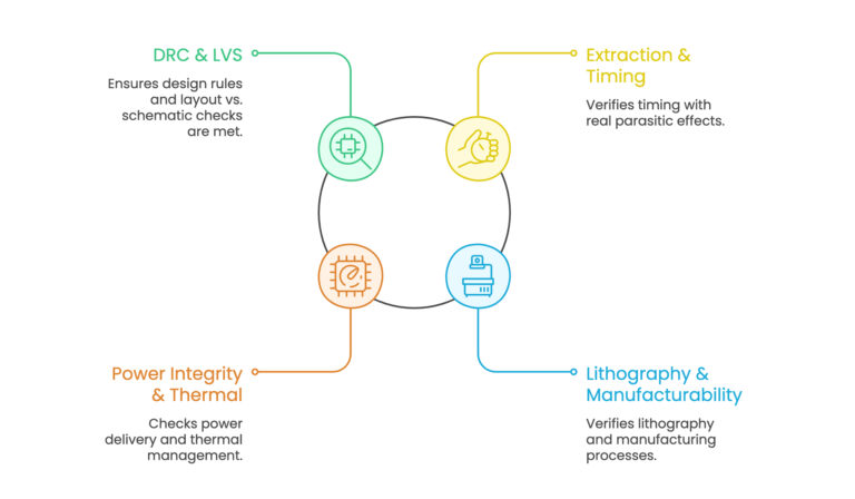
Signoff is no longer a static checklist. It has evolved into a full pipeline that validates logical intent, physical correctness, manufacturability, and test readiness.
1. DRC & LVS: The Non-Negotiables
Beyond standard rule decks, advanced nodes now require:
- Multi-patterning checks
- Fin width/height compliance
- Advanced via enclosure rules
- Density rule compliance for uniform lithography
Integrating these into nightly regressions reduces surprises during final signoff.
2. Extraction & Timing with Real Parasitics
As routing complexity increases, accurate parasitics become essential. Modern SoCs require:
- Multi-corner extraction
- Crosstalk-aware STA
- EM-aware timing derates
This ensures timing margins remain realistic across voltage, temperature, and aging conditions.
3. Power Integrity & Thermal Checks
Tape-out signoff now includes:
- Dynamic IR-drop simulations
- Power-grid robustness
- Thermal hotspot prediction
- Clock tree EM aging
These steps prevent silicon-level reliability issues that may appear months after production.
4. Lithography & Manufacturability Verification
For 7nm and below, manufacturability signoff is critical. This includes:
- OPC/RET simulation
- Litho hotspot scanning
- Pattern-matching checks
- Density uniformity validation
These checks ensure the GDSII data translates into shapes that are actually manufacturable on silicon.
Strengthening Data Integrity Across Layout and Verification Teams
Data integrity is often the silent failure point in SoC programs. Even minor inconsistencies at the layout level can cascade into signoff delays, integration conflicts, or silicon defects. Implementing structured data control practices not only improves accuracy but also delivers measurable gains in tape-out efficiency and predictability.
1. Use a Hierarchical Data Management Approach
Track changes at the:
- Cell level
- Block level
- Full-chip level
This structured approach enables precise visibility into where violations originate and simplifies cross-team coordination during integration.
Impact on Program Outcomes:
- Reduces debug and violation isolation time by 20–30% through faster root-cause identification
- Enables parallel verification across blocks, accelerating overall signoff timelines
- Improves traceability across revisions, minimizing integration conflicts
Net Result: Faster signoff convergence and reduced risk of late-stage design surprises
2. Enforce GDS Lockdown Policies
Once blocks pass signoff, lock them to prevent accidental or unauthorized modifications. Maintaining a “golden” GDS for each block ensures consistency across all downstream processes.
Impact on Program Outcomes:
- Reduces last-minute regressions by 30–50% by preventing unintended post-signoff changes
- Ensures alignment between verified and released layout data
- Minimizes instability caused by late ECO cycles
Net Result: Higher first-pass tape-out success and lower probability of costly re-spins
3. Automate GDS Diff and Visualization
Use automated tools to compare GDS versions and visually highlight differences such as:
- Missing vias
- Layer misalignment
- Hierarchy inconsistencies
- Metal density deviations
Impact on Program Outcomes:
- Cuts manual review effort by 40–60%, improving engineering productivity
- Detects critical discrepancies early in the flow, before signoff closure
- Accelerates validation of iterative design changes
Net Result: Shorter verification cycles and improved layout accuracy before tape-out
Improving Handoff Quality for Foundry Tape-Out
Before submitting to the foundry, a clean tape-out package must include:
- Verified GDSII or OASIS layout
- Runset versions and signoff reports
- Layer mapping files
- OPC-ready mask preparation data
- Fill/density reports
- Timing & power signoff summaries
- DFT, ATPG, and coverage data
- Constraints and ECO history logs
Foundries treat incomplete or inconsistent files as a major risk. leading to delays. Ensuring artifact completeness is one of the biggest responsibilities for anyone offering chip design services.
Reducing Re-Spins Through Smart Workflow Practices
A small but strategic improvement in workflow can drastically reduce tape-out risk:
- Run pre-tape-out mock cycles to validate handoff scripts.
- Use small “sanity test” designs to verify PDK or tool version changes.
- Maintain version-stamped signoff snapshots so debugging becomes traceable.
- Add “layout freeze” periods to avoid unnecessary late ECO churn.
These practices create predictable and stable conditions for a clean tape-out.
From Concept to GDSII: A Deep Dive into the VLSI Design Flow
People, Teams, and Shared Accountability
The last 5% of tape-out work is often the hardest because responsibility becomes shared across many teams, including physical design, DFT, timing, analog, packaging, and test. Clear ownership roles and cross-team alignment meetings prevent bottlenecks. Encouraging an early escalation culture helps uncover hidden issues before they become critical.
Tessolve: Your End-to-End Silicon Partner
At Tessolve, we’ve spent over two decades guiding customers from architecture to full productization, combining chip design expertise with deep test engineering and advanced SoC validation capabilities. Our end-to-end model spans RTL, physical design, DFT, package co-design, test program development, failure analysis, and full product qualification. As one of the most trusted chip design companies, we prioritize data integrity through manifest-driven workflows, rigorous signoff methodologies, and seamless tape-out support. With our in-house ATE labs, reliability centers, and strong foundry partnerships, we ensure predictable tape-out success and accelerated post-silicon debug, delivering silicon that works, the first time.
Frequently Asked Questions (FAQs)
1. What is the role of GDSII in the SoC tape-out process?
GDSII provides the final mask-ready layout data, ensuring all physical, hierarchical, and manufacturability elements are accurately represented for fabrication.
2. Why is layout signoff essential before submitting a design to the foundry?
Layout signoff verifies DRC, LVS, timing, power integrity, and manufacturability checks to prevent costly silicon failures and re-spins.
3. How do engineering teams maintain data integrity during final layout preparation?
Teams use controlled repositories, checksum validation, automated regressions, and strict versioning to keep layout data consistent across revisions.
4. What challenges arise when merging multiple GDS files for complex SoCs?
GDS merges often create hierarchy conflicts, missing references, density mismatches, and layer inconsistencies, requiring automated diff and validation tools.
5. How can tape-out delays be minimized in large chip design programs?
Automated signoff flows, early physical verification, strong cross-team coordination, and clear ownership reduce last-minute ECO cycles and delays.