
The field of semiconductor technology is in a perpetual state of advancement, spurred by the growing need for more efficient, powerful, and compact electronic devices. Today, advancements in AI, automotive electronics, 5G, IoT, and high-performance computing are accelerating the demand for increasingly sophisticated semiconductor solutions. A key aspect of this advancement is the complex process of Very Large Scale Integration (VLSI), which enables the creation of advanced Integrated Circuits (ICs) used in a wide range of applications, from smartphones to supercomputers.
The journey from an initial idea to a fully functional IC, ultimately represented in the GDSII format, follows a well-defined and intricate design flow. This article thoroughly examines each phase of the VLSI design flow, highlighting the essential steps needed to turn a concept into a tangible product.
1. Conceptualization and Specification
Every chip design begins with a concept. Whether driven by market needs, innovation, or specific requirements from “chip design companies,” this stage involves defining the purpose and functionality of the IC. Detailed specifications are drawn up, covering aspects like performance targets, power consumption, area constraints, and cost considerations. Modern chip specifications also account for security, scalability, functional safety, and manufacturability from the earliest design stages. These specifications serve as the blueprint for the VLSI design process.
At this stage, the VLSI board design is considered part of the more extensive system in which the chip will operate. Integrating the chip design with the overall board design ensures compatibility and functionality within the final product.
2. RTL Design and Verification
Once the specifications are clear, the next step is implementing that idea into an RTL design using hardware description languages such as Verilog or VHDL. At this stage, a high-level representation of the circuit is developed, focusing on data flow and control logic with respect to signals’ timing. The RTL design is actually a crucial step in the VLSI design flow that sets up the stage for a physical implementation.
At this stage, verification is performed in parallel and is equally important. The RTL design must be verified to ensure that it works correctly under different conditions using simulation, formal verification, and coverage-driven methodologies. This step detects functional errors in the VLSI design process early, reducing costly design iterations later in the flow.
3. Logic Synthesis
Logic synthesis converts the RTL design into a gate-level netlist, which represents the circuit using logic gates and flip-flops. This step marks the transition of abstract design into its concrete realization. The synthesized design must adhere to timing, power, and area constraints stipulated during the specification phase. At this stage, VLSI design tools optimize the netlist for Power, Performance, and Area (PPA) so that the resultant product can compete with several solutions offered by chip design companies.
4. Physical Design
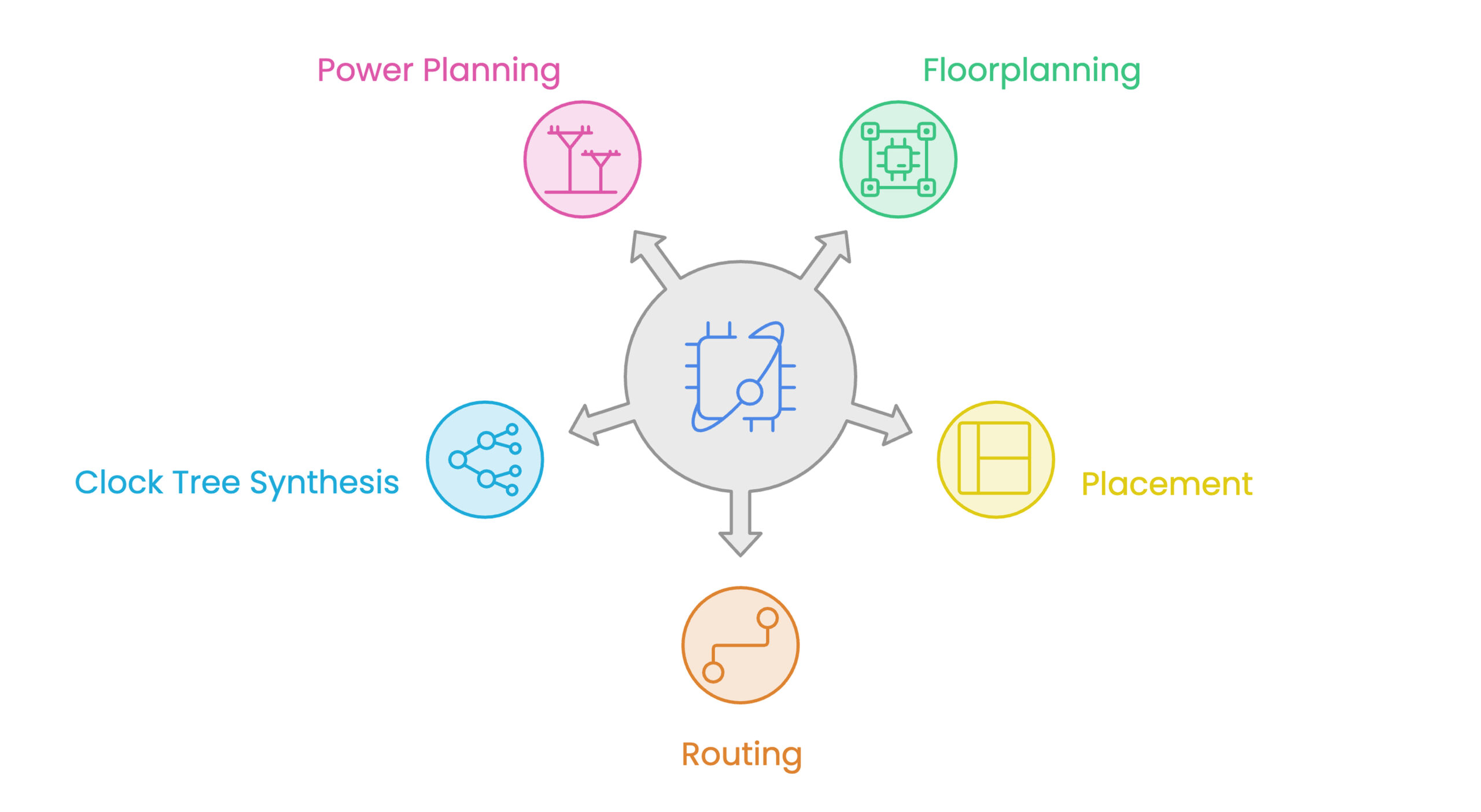
Physical design, also known as VLSI physical design, is where the design moves from the digital domain to the physical domain. This stage involves several key steps:
- Floorplanning: The chip area is divided into blocks to minimize wire length and optimize performance.
- Placement: Components (standard cells) are placed within the designated blocks.
- Routing: Electrical connections between the components are established.
- Clock Tree Synthesis (CTS): The clock distribution network is designed to minimize clock skew and jitter.
- Power Planning: Power distribution networks are optimized to ensure stable voltage delivery and reduce IR drop across the chip.
Physical design is one of the most critical stages in the VLSI design flow. It directly impacts the manufacturability, performance, and power consumption of the final chip. At this stage, VLSI solutions, including advanced routing algorithms and design rule checks (DRC), come into play to ensure that the design is functional and manufacturable.
5. Design for Testability (DFT)
Before moving towards fabrication, it’s essential to incorporate test structures within the design. DFT techniques ensure that the chip can be tested for defects after manufacturing. This step adds extra layers of assurance, allowing chip design companies to maintain quality control and reduce the risk of costly post-production failures. Modern DFT techniques include scan insertion, Built-In Self-Test (BIST), Memory BIST (MBIST), and boundary scan to improve fault coverage while reducing test time and manufacturing costs.
Download Brochure
Accelerate your VLSI journey with Tessolve’s VLSI chip designs and engineering services
Case Study PDF Download
6. Timing Analysis and Power Optimization
Timing analysis, particularly Static Timing Analysis (STA), ensures that the design meets the required timing constraints. Power optimization is performed in tandem, focusing on reducing both dynamic and static power consumption. These steps are vital to ensure that the chip meets the performance and efficiency targets set during the specification phase.
VLSI physical design is crucial as the chip’s layout affects timing and power consumption. Tools in this phase offer insights for optimization, while techniques such as clock gating, power gating, multi-voltage domains, and Dynamic Voltage and Frequency Scaling (DVFS) enhance power efficiency.
7. Layout Verification
Once the physical design is complete, the layout is verified against the original netlist to ensure accuracy. Design Rule Checking (DRC) and Layout vs. Schematic (LVS) checks are performed to confirm that the design adheres to the manufacturing process rules and that the layout matches the intended circuit.
VLSI solutions that automate these verification processes are crucial at this stage, enabling rapid and accurate checks that minimize the risk of errors slipping through to the final stages of the VLSI design flow.
8. GDSII Generation
The final step in the VLSI design flow is the generation of the GDSII file, which is the standard format used for IC manufacturing. This file contains all the information needed to produce the physical chip, including layer information, geometric shapes, and connectivity data. The GDSII file is handed over to the foundry for fabrication, marking the transition from design to production. Following successful sign-off, the design proceeds to tape-out, where the finalized GDSII database is released for semiconductor fabrication.
The Rise of mmWave Technology: Enabling High-Speed Wireless in Automobiles
Let’s Conclude
The progression from concept to GDSII in VLSI design is a multifaceted, meticulously detailed process that requires the concerted use of various tools, methodologies, and skilled professionals. Each stage plays a pivotal role in shaping the end product, from the initial VLSI board design to the ultimate physical layout. The continuous evolution of VLSI solutions enables swifter, more effective design processes that meet the burgeoning requirements of the technology sector. Chip design companies rely on this resilient VLSI design flow to deliver pioneering, high-performance chips that drive the next era of electronic devices.
Comprehending the VLSI design flow is imperative for anyone engaged in semiconductor design and manufacturing. Whether an individual is a student, an engineer, or an enthusiast, delving deeply into this process offers invaluable insights into the creation of the chips propelling modern technology.
FAQs
1. What is the VLSI design flow?
The VLSI design flow transforms chip concepts into manufacturable ICs through specification, RTL design, synthesis, physical design, verification, and GDSII generation.
2. What is GDSII in VLSI?
GDSII is the standard file format containing a chip’s physical layout data, used by semiconductor foundries for IC fabrication.
3. What is the full form of GDSII?
GDSII stands for Graphic Data System II, the industry-standard layout database format used for integrated circuit manufacturing.
4. What are the main steps in the VLSI design flow?
The VLSI design flow includes specification, RTL design, verification, synthesis, physical design, DFT, timing analysis, layout verification, and GDSII generation.
5. What is the difference between GDS and GDSII?
GDS is the original Graphic Data System, while GDSII is its enhanced version and the industry standard for IC layout exchange.