A reliable power distribution network (PDN) is the backbone of every printed circuit board (PCB). If power delivery is unstable, even the most advanced PCB design can fail due to voltage drop, noise, or IR drop issues. This article explains what a PDN is, why it matters, and how to design it efficiently to ensure stable power delivery for your electronic systems.
What is a Power Distribution Network (PDN)?
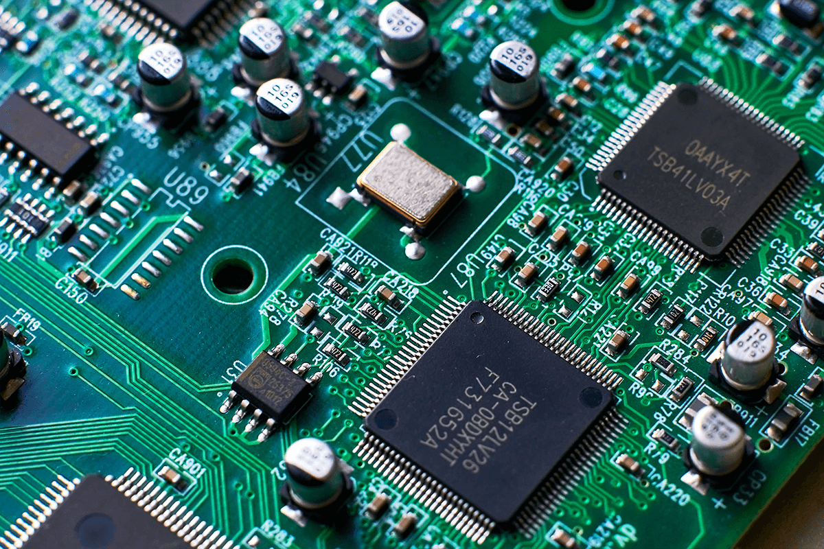
A Power Distribution Network (PDN) is the network of power and ground connections that deliver power from the source (like VRMs or batteries) to every IC and component on the PCB.
Its role in PCB design is to:
- Maintain a steady voltage across the board.
- Minimize IR drop and power noise.
- Provide low-impedance paths for transient current demands.
Example use cases include high-speed digital boards, RF systems, and automotive ECUs where power integrity is mission-critical.
PDN Simulation Tools & Techniques
Simulation plays a key role in predicting PDN behavior before fabrication. Tools such as PowerSI, Cadence Sigrity, and Ansys SIwave allow designers to model voltage drop, current density, and impedance profile across frequencies. This ensures power integrity and helps optimize capacitor selection and placement.
Consequences of Poor PDN Design
- Voltage Droops:
Inadequate power distribution can result in voltage drops. The voltage supplied to components can temporarily decrease during high-current demand, leading to malfunction or data corruption. - Noise Interference:
Poor PDN design can introduce noise into the power supply. This can cause fluctuations in voltage levels and disrupt the functionality of sensitive components. The noise can propagate through the circuit and can affect signal integrity and overall performance. - Signal Integrity Issues:
Unstable power delivery can manifest as signal integrity issues, such as ringing, overshooting, and undershooting. This compromises the accuracy and reliability of data transmission within the circuit.
Introduction to PCB Power Distribution Networks (PDN)
Semiconductor devices require adequate power to function correctly. However, ensuring efficient power delivery poses a complex and costly challenge in electronics design.
It typically begins with a power supply transmitting power via wires to a PCB board. On this board, one or more integrated circuits (ICs) are affixed. Copper Traces on the PCB connect from the pads, where power supply wires are linked, to the pads that transfer power to the chip. These traces may utilize vias to traverse through the PCB board. Connecting from the chip pad to the chip involves pins or bumps that link to the semiconductor surface, often using wires or other conductive materials soldered in place. Subsequently, a network of metal layer traces, vias, and potential traces within the silicon connect the transistors to the power supply. However, this pathway inherits resistances, capacitances, and inductances, resulting in variations from the original power supply output at the transistor.
To ensure proper voltage levels for different components of the circuit, voltage regulators or converters may be strategically inserted along this pathway. In low-power designs, switches within the power supply may exist to selectively power down sections of the circuit, reducing leakage power. Additionally, capacitors may be included to store enough charge to meet instantaneous demand during peak current demands, subsequently recharging during periods of lower current requirements.
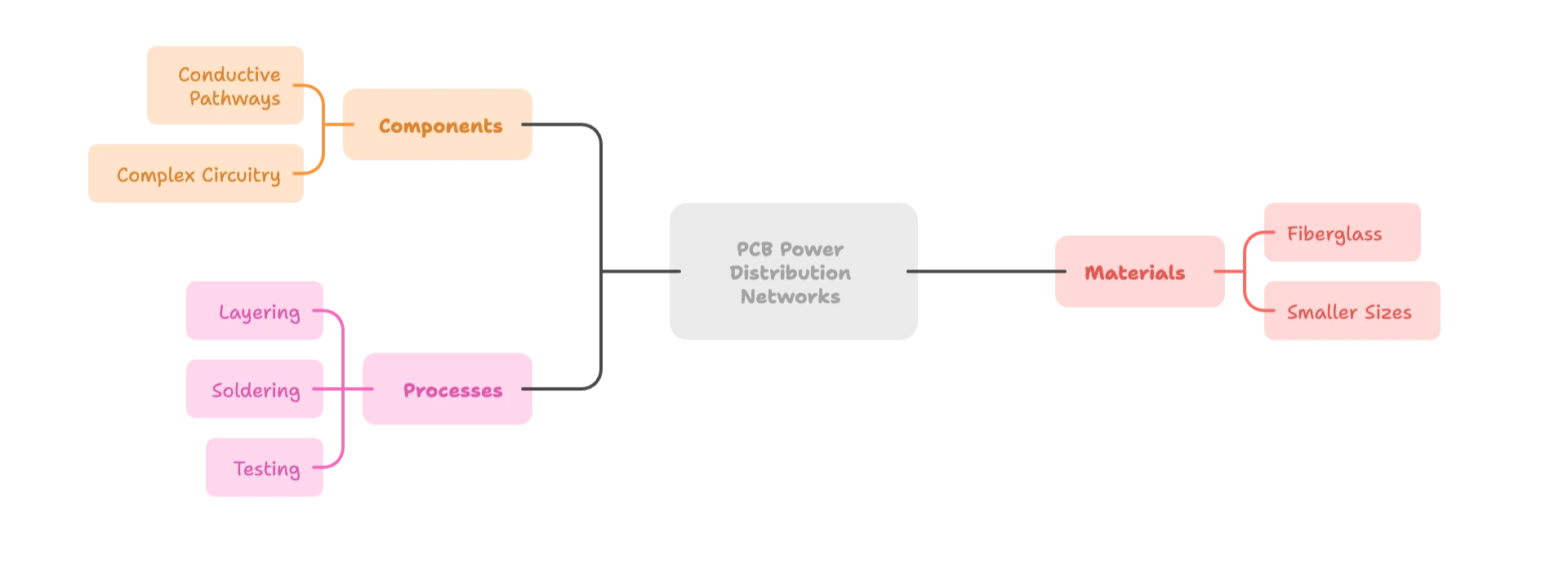
The PDN encompasses a network of traces, planes, and components designed to deliver power from the primary source to individual components. It plays a fundamental role in maintaining the stability and reliability of electronic circuits by supplying consistent and clean power. Without a well-designed PDN, electronic devices may experience operational issues, including erratic behavior, data corruption, and even system failures.
Designing an efficient and reliable PDN is paramount in PCB design. It involves meticulous planning and optimization to ensure proper power distribution and minimal interference. By focusing on PDN design, engineers can enhance the performance, longevity, and overall quality of electronic devices.
Why Stable Power Delivery Is Critical in PCB Design
Stable power delivery is vital for an electronic device to ensure that components receive the required voltage and current levels. This helps to operate devices within their specified parameters. Any deviation from the expected power supply can have profound effects on circuit performance and reliability.
Consider a scenario where a voltage spike occurs due to insufficient decoupling or poor PDN design. It can affect the device and lead to the malfunctioning of chips. Similarly, voltage sags caused by inadequate power distribution can lead to signal degradation and data corruption. This can impact the overall functionality of the device.
Moreover, an unstable power supply to PCB can introduce noise and interference into the system. This can affect signal integrity and cause electromagnetic compatibility (EMC) issues. This can be problematic in high-frequency applications or environments with stringent EMC requirements.
Effective PDN design is crucial to mitigate these risks. By optimizing the layout and configuration of the PDN components, engineers can minimize noise, voltage drops, and other power-related issues. This ensures that electronic devices operate reliably under various operating conditions, enhancing their overall performance and longevity.
Best Practices for Effective Power Distribution Network

The PDN comprises several key components, each serving a specific function in ensuring efficient power distribution and noise suppression:
- Power sources:
These are the leading suppliers of power to the PCB design board, consisting of batteries, power supplies, or external sources. - Traces:
Traces are conductive pathways that route power from the sources to individual components on the PCB design board. They play a crucial role in delivering power efficiently while minimizing impedance and voltage drops. - Planes: PCB board
planes are large copper areas on the board that act as low-impedance paths for power distribution. They provide a stable ground reference and help distribute power evenly across the board. - Decoupling Capacitors:
Decoupling capacitors are strategically placed throughout the PDN to absorb high-frequency noise and provide local energy storage. They help stabilize voltage levels and reduce voltage fluctuations caused by sudden changes in current demand. - Voltage Regulators:
Voltage regulators control and regulate the voltage levels to ensure consistent power supply to sensitive components. They help maintain voltage stability, even in the presence of varying input voltages or load conditions.
What Are the Challenges of Signal Integrity in High-Speed PCB Design?
Decoupling Capacitors in PDN Design: Strategies for Effective Bypassing
In the intricate landscape of PCB design, power integrity stands as a crucial aspect governing the reliability and performance of electronic systems. You can’t overstate the importance of stable power delivery to sensitive electronic components while designing a custom PCB board. This is essential for optimal performance and reliability. At the heart of power integrity lie two indispensable components: bypass capacitors and decoupling capacitors. While these capacitors are often conflated or their roles misunderstood, it’s imperative to discern their distinct functions and their impact on mitigating power integrity issues.
Two Related Power Integrity Problems
Decoupling capacitors and bypass capacitors are instrumental in addressing distinct yet interrelated power integrity challenges. Despite their terminology, which might imply diversion, these capacitors operate within the PDN to counteract voltage fluctuations and maintain signal integrity. The fundamental distinction lies in the fluctuations they mitigate and their placement within the circuit.
Role of Decoupling Capacitors in PDN Design
Decoupling capacitors helps reserve energy within the PDN. This enables instantaneous power to integrated circuits (ICs) while mitigating voltage fluctuations and noise. These capacitors act as a buffer, absorbing and releasing charge as needed to stabilize voltage levels and maintain signal integrity. Their placement near the power pins of ICs minimizes the inductance of the power delivery path, ensuring rapid response to transient currents and reducing voltage droops.
Strategies for Effective Bypassing
- Placing Capacitors Close to Power Pins:
Proximity is critical in bypassing strategies. It reduces the inductance between capacitors and ICs and improves their effectiveness in filtering out noise. By placing decoupling capacitors closer to the power pins of ICs, a hardware designer minimizes the loop area and inductance. This can enhance noise suppression. - Using a Combination of Capacitor Values:
Employing capacitors with different values addresses a broader frequency range of noise. This enhances the PDN’s noise suppression capabilities across various frequencies. This also allows a hardware designer to target specific frequency ranges of noise and improve overall noise reduction. - Implementing Multiple Layers of Decoupling Capacitors:
A hardware design engineer can utilize capacitors with varying capacitance values on different layers of the PCB design board. This helps to optimize the PDN’s response to different frequency components of noise. Additionally, it allows for distributed capacitance, helping to reduce the overall impedance of the PDN and improve noise filtering performance. - Employing Distributed Capacitance:
Strategically placing capacitors throughout the PCB board creates a network of low-impedance paths. This reduces inductance and improves the PDN’s overall impedance profile. Moreover, it helps a hardware designer minimize voltage fluctuations and to ensure a stable power delivery network. - Selection Criteria for Decoupling Capacitors:
Capacitance value, voltage rating, and Equivalent Series Resistance (ESR) are critical factors to consider when choosing decoupling capacitors. High capacitance values and low ESR are desirable for effective noise filtering and voltage stabilization. Additionally, selecting capacitors with appropriate voltage ratings ensures reliability and longevity in operation.
PCB Design Basics: A Comprehensive Guide for Beginners
Introduction to PCB Design Principles
PCB design involves a collaborative effort across various disciplines like electrical, mechanical, and software engineering to create printed circuit boards. It consists of conductive and insulating layers, with copper traces etched onto the conductive layers. Components are soldered onto pads on the outer layers, with vias allowing interconnections between layers. The custom PCB board is widely used due to automation in manufacturing, offering cost-effective and efficient circuit production compared to alternative methods like wire wrap.
Additionally, today’s electronics design landscape demands a streamlined approach to tackle complexity and tight schedules. Providing teams with collaborative tools and comprehensive solutions enables them to thrive in this demanding environment, fostering innovation and efficiency in electronic systems design.
PCB design is essential for the following reasons:
- PCB board design offers an organized framework for signal routing and component connections, ensuring the dependable and effective operation of electronic equipment.
- Smaller, more portable electronic devices are made possible by the compact integration of electronic components made possible by a PCB design board.
- Effective PCB board design raises the overall reliability of electronic systems by lowering the chance of electrical shorts, signal interference, and component failures.
- For electronic products, an efficient PCB board design shortens the time to market and lowers production costs.
Role of PCBs in Electronic Devices
- Component Mounting: Printed circuit boards offer a surface on which electronic components can be mounted and connected.
- Electrical Connections: Through the use of conductive traces and vias, a PCB board enables the routing of electrical impulses between components, guaranteeing appropriate communication within the circuit.
- Signal Integrity: A custom PCB board contributes to the preservation of signal integrity by reducing crosstalk, impedance mismatches, and EMI.
- Thermal Management: PCB design board allows the incorporation of thermal vias, copper pours, and heatsinks, helping dissipate heat produced by electronic components.Overview of PCB Design Process
- Requirements Analysis: Identify the functional requirements, performance specifications, and constraints for the design PCB.
- Schematic Design: Create a schematic diagram representing the electrical connections and component placements.
- Component Placement: Arrange electronic components on the PCB layout according to the schematic design and mechanical constraints.
- Routing: Establish electrical connections between components by routing traces on the PCB board, considering signal integrity, power distribution, and thermal management.
- Design Verification: Perform design rule checks (DRC) and electrical simulations to validate the integrity and functionality of the PCB layout.
- Prototyping: Fabricate a prototype PCB to verify performance and functionality through testing and debugging.
- Manufacturing: Prepare the design PCB files for production, including fabrication, assembly, and testing processes.
- Quality Assurance: Conduct quality inspections and testing to ensure the manufactured PCB board meets the desired specifications and standards.
Basic Concepts in PCB Design
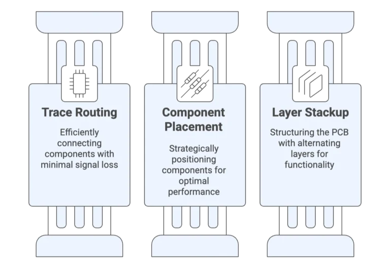
Trace Routing
Traces are thin copper lines on the PCB design board that connect various components electrically. They carry signals and power between components. Its width depends on current, signal frequency, and desired impedance. Its minimized length for high-speed signals reduces signal integrity issues. It supports orthogonal routing, curved traces, minimizing vias, routing techniques, etc.
Component Placement
Careful placement impacts performance, manufacturability, and thermal management. Place critical components close together for better signal integrity. Place heat-generating components near heat sinks or ventilation holes. Isolate EMI-sensitive components from noise sources. Minimize stress on components while mounting due to board flex.
Layer Stackup
The structure of the PCB board consists of alternating layers of dielectric and conductive materials. The custom PCB board consists of single, double, or multiple layers, with each layer serving a specific purpose in the overall design. The layer stack-up determines the PCB’s routing capabilities, signal integrity, and manufacturing complexity. Leverage power and ground planes provide stable power and reference potential. Additionally, use internal planes for complex designs with high-speed signals.
While designing a custom PCB board, consider the number of layers based on complexity and signal requirements. Ensure stack-up order to optimize signal integrity and minimize crosstalk.
Additional Important Concepts
- Grounding: Proper grounding is crucial for signal integrity and noise reduction.
- Decoupling capacitors: Suppress power supply noise across the board.
- Soldermask and silkscreen: Provide protection and component identification.
- Design rule checking (DRC): Ensures layout adheres to manufacturing limitations.
Familiar PCB Design Software Tools
PCB hardware design software helps you create the physical layout and schematics of PCB. They offer various features and tools to streamline the design process, from the initial concept to the final Gerber files for manufacturing.
There are different types of PCB hardware design software available, categorized by their complexity, features, and price point.
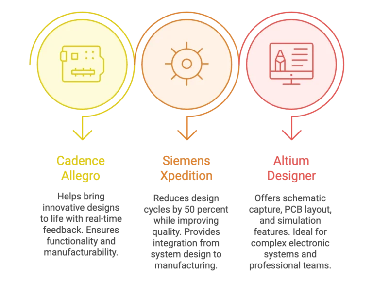
- Cadence – Allegro: Cadence Allegro PCB Design helps bring your innovative and bleeding-edge designs to life. The constraint-driven environment provides real-time visual feedback and ensures the functionality and manufacturability of your PCBs while allowing you to keep designing.
- Siemens – Xpedition: Xpedition Enterprise is the industry’s most innovative PCB design flow, providing integration from system design definition to manufacturing execution. Its unique technologies can reduce design cycles by 50 percent or more while significantly improving overall quality and resource efficiency.
- Altium Designer: It is a comprehensive PCB design software offering schematic capture, PCB layout, and simulation features. It provides advanced capabilities for high-speed PCB board design, rigid-flex design, and multi-board assembly. This makes it ideal for complex electronic systems and professional design teams.
Getting Started with PCB Design
Schematic Design
- Learn about essential electronic components like resistors, capacitors, transistors, and integrated circuits. Familiarize yourself with reading and interpreting datasheets.
- Grasp the relationship between schematics, which represent the circuit’s connections, and PCB layout, which physically implements them on the board.
- Choose beginner-friendly software like KiCad, EasyEDA, or Fritzing. Learn the basic functionalities for creating schematics and layouts.
- Understand factors like trace width, spacing, and layer stack-up that impact signal integrity and board manufacturability.
Practical steps
- Begin with a primary circuit like a blinking LED or a simple amplifier to practice the design flow.
- Draw your circuit using symbols and connections accurately reflecting your desired functionality.
- Place components logically considering thermal dissipation, signal routing, and ease of assembly.
- Connect components with traces adhering to design rules and ensuring signal integrity.
- Validate your design for adherence to rules and potential electrical issues.
- Export your design files in Gerber format for manufacturing.
Advance in PCB Design Techniques
- High-speed design: Understand signal integrity principles, transmission lines, and impedance control for high-frequency circuits.
- Multi-layer boards: Utilize multiple layers for complex designs, addressing signal routing challenges and power delivery needs.
- EMI/EMC considerations: Implement strategies to mitigate electromagnetic interference and ensure regulatory compliance.
- Advanced component integration: Integrate ball grid arrays (BGAs), fine-pitch components, and flexible circuits into your designs.
- Design for manufacturability (DFM): Consider manufacturing limitations and optimize your design for cost-effective production.
PCB Design Best Practices
- Plan and document clearly: Define project requirements, create clear schematics and layouts, and maintain detailed documentation.
- Prioritize signal integrity: Minimize trace length, avoid sharp bends, and ensure proper impedance matching for high-speed signals.
- Thermal management: Consider component heat dissipation and implement heat sinks or copper pours for efficient cooling.
- Component placement and routing: Place components logically for the shortest possible connections and maintain good signal flow.
- Decoupling and power integrity: Use decoupling capacitors to suppress noise and ensure consistent power supply to all components.
- Grounding and shielding: Implement proper grounding practices and consider shielding sensitive components for EMI mitigation.
- Design for testability: Include test points and consider designing test fixtures for easier troubleshooting.
- Version control and revision management: Track design changes and maintain clear versions for effective collaboration.
The Role of Enterprise Hardware Solutions in Supporting Your IT Infrastructure
Advanced PCB Design Techniques: Pushing the Boundaries of Innovation
Advanced PCB hardware design isn’t just complex boards; it’s an innovation engine. Shrinking devices, boosting performance, and cramming in features – that’s what it does. High-speed signals, multi-layers, and fancy components are all controlled for perfect performance and manufacturability. Advanced PCB board design paves the way for smaller, faster, and latest-generation electronic devices.
What Are the Advanced PCB Design Methodologies?
HDI (High-Density Interconnect)
HDI technology increases routing density and smaller form factors, making it ideal for compact electronic devices.
Advantages:
- Enhanced signal integrity and reliability due to shorter signal paths and reduced electromagnetic interference.
- Ability to accommodate high pin-count components and complex circuitry, leading to improved functionality.
Challenges:
- Higher manufacturing costs are associated with advanced fabrication processes such as laser drilling and sequential lamination.
- Increased design complexity, requiring careful consideration of signal routing, power distribution, and thermal management.
Flex-Rigid PCBs
Flex-rigid PCBs combine flexible circuits’ flexibility with rigid boards’ structural integrity, offering unique design possibilities.
Advantages:
- Reduced space and weight compared to traditional PCBs, making them suitable for compact and lightweight devices.
- Improved reliability and durability, as flex-rigid constructions eliminate the need for connectors and solder joints.
Challenges:
- Complex design and manufacturing processes require flexible and rigid PCB technology expertise.
- Limited availability of materials and fabrication capabilities, leading to higher production costs.
RF/Microwave PCBs
RF/microwave PCB board is optimized for high-frequency applications like wireless communication, radar systems, and satellite communication.
Advantages:
- Low signal loss and impedance matching capabilities are essential for maintaining signal integrity at high frequencies.
- Precise control over dielectric properties and conductor geometries, enabling efficient transmission and reception of RF signals.
Challenges:
- Tight design tolerances and strict manufacturing requirements ensure accurate signal propagation and minimal signal degradation.
- Limited availability of specialized materials and fabrication techniques leads to higher production costs and longer lead times.
High-Performance Signal Management
Controlled Impedance Techniques:
- Achieve controlled impedance by defining trace width, spacing, and dielectric material properties. Discuss design tools and calculators for accurate impedance calculations.
- Maintain consistent signal strength and minimize noise by routing balanced differential pairs with controlled spacing and equal lengths.
- Before fabrication, utilize advanced simulation software like Ansys HFSS or HyperLynx to analyze signal reflections, crosstalk, and timing violations.
Advanced Routing Algorithms:
- Automatically adjust trace lengths to minimize signal skew and ensure simultaneous destination arrival.
- Discuss trade-offs between shortest routing for minimal delay and maintaining controlled impedance for signal integrity.
- Utilize via placement and layer changes effectively to optimize signal routing in complex multi-layer boards.
Pre-fabrication Verification:
- Validate signal integrity, power delivery, and thermal performance using advanced simulation tools before committing to fabrication.
- Ensure your design adheres to manufacturing guidelines and electrical rules to avoid costly errors.
- Build and test prototypes with representative components to verify functionality and performance before mass production.
Multi-Layer Mastery
- Design with controlled impedance layers, dedicated power, ground planes, and isolation layers to minimize noise and crosstalk.
- Incorporate thermal planes or strategically placed vias for efficient heat dissipation in densely packed boards.
- Balance layer counts with performance needs while considering fabrication limitations and cost implications.
Blind and Buried Vias:
- Utilize blind and buried vias for shorter connections within inner layers, reducing signal length and improving signal integrity.
- Achieve higher density routing by eliminating vias on outer layers, leading to smaller board footprints.
- Understand the higher cost and complexity of blind and buried vias than through-hole vias.
Embedded Components:
- Embed capacitors and resistors within the PCB dielectric for space optimization and improved high-frequency performance.
- Consider the potential impact on signal integrity and thermal management when embedding components.
EMI/EMC Control Strategies Shielding Techniques:
- Enclose sensitive components or entire boards with conductive shields to block external electromagnetic interference (EMI).
- Choose components with inherent shielding properties or integrate EMI filters for added protection.
- Implement proper grounding and isolation techniques to minimize noise coupling and signal disturbances.
Grounding Practices:
- Utilize a single reference point for grounding to minimize ground loops and potential noise issues.
- Connect components directly to a central ground point for improved noise reduction and signal integrity.
- Ensure dedicated and low-impedance paths for current return to minimize interference with signal traces.
Layout Strategies for Compliance:
- Design your PCB layout to comply with relevant EMI/EMC standards like FCC or CE marking.
- Utilize filtering techniques, shielding, and proper component selection to reduce radiated emissions from your PCB.
- Design for immunity to external EMI by implementing proper grounding and filtering strategies.
Advanced Component Integration
Ball Grid Arrays (BGAs) and Fine-pitch Components:
- Enable smaller board footprints and increased functionality by incorporating BGAs and fine-pitch components with smaller footprints.
- Due to smaller package sizes, address challenges like solder joint reliability, thermal management, and high-frequency signal integrity.
- Understand the need for specialized assembly techniques like solder paste jetting and automated placement for high-density components.
Flexible Circuits and Rigid-flex Boards:
- Utilize flexible circuits for wearable electronics, medical devices, and other applications requiring conformability or flexure.
- Address challenges like mechanical stress, fatigue, and signal integrity in flexible sections.
- Understand the specialized fabrication processes involved in producing flexible and rigid-flex PCBs.
DFM for Manufacturability and Reliability
Design Guidelines for Assembly and Soldering:
- Consider pick-and-place accessibility, hand soldering feasibility, and thermal management when placing components.
- Choose standard footprints compatible with common assembly processes and component availability.
- Optimize solder joint geometry for strength, reliability, and compatibility with specific soldering techniques.
- Allow sufficient clearance between components and traces for assembly and component tolerances.
- Design for ease of manual or automated assembly, considering factors like screw access, connector placement, and cable routing.
Thermal Management Strategies:
- Identify significant heat sources like power ICs and high-current components.
- Utilize heat sinks, strategically placed vias, and copper ground planes for efficient heat dissipation.
- Choose low-power components whenever possible and consider thermal ratings when selecting others.
- Design for adequate airflow in enclosed systems to remove heat.
- Utilize simulation tools to analyze thermal distribution and identify potential hotspots before fabrication.
Design for Testability (DFT) Methodologies:
- Include dedicated test points on the PCB for easy electrical measurements and signal probing during testing.
- Incorporate test circuitry within the design to perform self-diagnostics and isolate potential failures.
- Implement boundary scan circuitry for easy access to internal nodes and on-chip testing capabilities.
- Utilize software tools to analyze DFT coverage and identify areas for improvement before fabrication.
PCB Layout for High-Frequency Applications: Challenges and Solutions
High-Speed PCB Design: Strategies for Signal Integrity and Transmission
High-speed PCB design ensures PCBs are capable of handling signals with rapid transitions and high frequencies. While seemingly mundane, it’s crucial for modern electronics, impacting countless industries and technologies.
Significance in modern electronics:
- Enables cutting-edge technologies: High-speed design PCB is essential for high-performance computing, advanced communication systems (5G, fiber optics), radar, and high-speed data acquisition. Achieving the raw data processing power and signal transmission speeds seen today wouldn’t be impossible without them.
- Maximizes performance and efficiency: High-speed IC Packaging Design ensures accurate data transmission, reduces power consumption and minimizes interference by addressing signal integrity concerns. This leads to more reliable and efficient electronic systems.
- Expands design possibilities: As technology miniaturization progresses, high-speed design expertise becomes vital in packing ever-increasing functionality onto smaller PCBs. This allows for compact and portable devices.
Considerations for Designing High-Speed PCBs
- Advanced Impedance Control
Precisely match the impedance of differential pairs to minimize skew between signals. It is crucial for maintaining data integrity at high speeds. Optimize the layer stack-up, including dielectric materials and layer thicknesses, to achieve the desired characteristic impedance and minimize crosstalk between layers.
- Advanced Routing Techniques
Utilize routing techniques, like serpentine routing and length-matched traces, to achieve equal lengths for differential pairs, ensuring signal arrival simultaneously. Minimize signal discontinuities and maintain controlled impedance using blind and buried vias instead of through-hole vias for signal paths.
- Advanced Noise Mitigation
Divide power planes into separate analog and digital circuits sections to reduce noise coupling between domains. Employ advanced SI analysis tools to accurately predict signal behavior, identify potential noise sources, and optimize the design for better performance.
- Thermal Management
High-speed components generate significant heat, potentially causing signal integrity issues. Implement heat sinks, fans, or other thermal management techniques to maintain optimal operating temperatures.
- Grounding and Power Distribution
Adequate grounding and power distribution are vital for minimizing ground bounce, voltage fluctuations, and noise in high-speed designs. Implement a solid ground plane, utilize power planes, and incorporate multiple ground vias to maintain stable power distribution and reduce signal crosstalk.
- EMI Management
High-speed PCBs are susceptible to electromagnetic interference (EMI), which can degrade signal quality and affect system performance. Shield sensitive components, use proper grounding techniques, and employ EMI filters to mitigate EMI issues and maintain signal integrity.
Optimal Approaches for Designing High-Speed Printed Circuit Boards
Strategies for Maintaining Signal Integrity
Maintaining signal integrity is critical in high-speed PCB design to ensure accurate and reliable data transmission. Several strategies are employed to preserve signal integrity effectively:
- Controlled Impedance Routing: Designing a transmission line with controlled impedance helps match the characteristic impedance of the traces to the system’s impedance requirements. This minimizes signal reflections and ensures optimal signal integrity throughout the PCB board in USA.
- Signal Termination: Proper termination techniques, such as series and parallel terminations, eliminate signal reflections at the ends of transmission lines. Termination resistors match the impedance of the transmission line, preventing signal distortion and maintaining signal integrity.
- Signal Length Matching: It is vital to minimize skew and timing mismatches. For this, one should ensure uniform signal propagation delays by matching the lengths of critical signal traces. This is particularly important for differential pairs and high-speed buses, where precise synchronization is essential for maintaining signal integrity.
- Layer Stackup Optimization: Careful planning of the PCB layer stackup is crucial for maintaining signal integrity. Use controlled impedance layers and minimize signal transitions between layers to reduce impedance variations and distortion, enhancing overall signal integrity.
- Grounding Techniques: Proper grounding techniques like star grounding and solid ground planes help minimize ground loops and reduce electromagnetic interference (EMI). A low-impedance ground reference is essential for maintaining signal integrity and reducing noise.
- Signal Integrity Analysis: A hardware design engineer can conduct a thorough signal integrity simulation and analysis using specialized software tools. This helps them identify and mitigate potential signal integrity issues early in the design phase. They should also analyze factors like impedance mismatches, crosstalk, and signal distortion to guide design decisions to optimize signal integrity.
- Via Design Optimization: A PCB engineering designer should optimize via placement and design to maintain signal integrity, especially in high-speed designs. They can use low-inductance vias and minimize signals via transitions. This reduces signal reflections and impedance disruptions and ensures consistent signal integrity.
- Shielding and EMI Mitigation: A hardware design services provider should employ shielding techniques and EMI mitigation strategies, such as ground stitching vias and shielded traces. This helps minimize electromagnetic interference and noise coupling. Additionally, it shields sensitive signals and components to preserve signal integrity and reduce the risk of data corruption.
EMC/EMI in PCB Design: Ensuring Compliance and Reducing Interference
Electromagnetic compatibility (EMC) ensures that the components and circuits on the board can coexist harmoniously without causing or being affected by unwanted electromagnetic disturbances. Achieving EMC is crucial to ensure electronic devices’ reliable and uninterrupted operation in various applications.
Electromagnetic interference (EMI) can disrupt electronic devices and systems, leading to performance degradation or malfunction. EMI disruption can have severe consequences for electronic devices and systems, including:
- Signal Distortion: Interference can distort signals, leading to data transmission and processing errors.
- System Instability: EMI-induced noise can destabilize circuits, causing erratic behavior or system crashes.
- Component Damage: High-intensity EMI can damage sensitive electronic components, leading to premature failure or permanent damage.
- Compliance Issues: Failure to meet EMC standards and regulatory requirements can result in product recalls, legal liabilities, and damage to brand reputation.
Regulatory Standards and Compliance
An electronic device should not be susceptible to EMI, and for this, it should be electronic-compatible. A PCB hardware designer can reduce EMI and increase EMC by following rules, regulations, and guidelines set by regulatory authorities. Additionally, designers should incorporate EMI reduction techniques in PCB power supply, such as EMI filtering, proper grounding, and more. Here’s a breakdown of common EMC standards, categorized by application:
- Medical Devices
IEC 60601-1-2: This paramount standard establishes safety and performance requirements for medical equipment in electromagnetic environments. Compliance ensures patient safety and proper functionality amidst potential interference.
- Automotive
SAE, ISO 7637, IEC CISPR-25, ISO 1145-1 & 2: These standards address testing procedures, measurement techniques, and limits for electromagnetic disturbances impacting automotive components. Adherence safeguards vehicle electronics and ensures reliable performance.
- Military Systems
MIL-STD-461, DEF STAN 59/411, MIL-STD-704, MIL-STD-1275, MIL-STD-1399: These stringent standards regulate electromagnetic emissions and susceptibility of military systems, guaranteeing operational integrity and resistance to interference in harsh environments.
- Industrial Equipment
FCC Part 15 Class A, EN 61000-6-4 (generic), EN 61000-6-2 (generic): These standards form a general framework for industrial devices, regulating intentional, unintentional, and incidental radiations. Compliance fosters a harmonious electromagnetic environment within industrial settings.
- Commercial Electronics
FCC Part 15 Class B, EN 61000-6-3 (generic), EN 61000-6-1 (generic): These standards define immunity requirements for commercial equipment in sensitive environments like residences and offices. Meeting these standards ensures compatibility and safe operation amidst various potential sources of interference.
Importance of Compliance:
- Meeting EMC/EMI standards ensures your product does not interfere with other devices or suffer from their interference, enhancing reliability and functionality.
- Excessive EMI can create electrical hazards or disrupt critical systems. Compliance minimizes these risks, ensuring user safety.
- Non-compliant products face market access restrictions, potential recalls, and legal repercussions. Compliance allows you to sell your product freely across regions.
- Demonstrating compliance through recognized certifications builds trust and reinforces the quality and safety of your product.
Techniques for EMI Reduction
- Grounding and Shielding
To minimize ground loops and reduce EMI, PCB engineering designers should utilize proper grounding practices such as star grounding and solid ground planes. They can effectively contain electromagnetic emissions and prevent external interference by implementing shielding enclosures, conductive coatings, and shielding materials.
- Signal Routing Optimization
Controlled impedance routing ensures consistent signal propagation and reduces signal reflections, minimizing EMI. Differential pair routing balances signal lines, mitigating common-mode noise and enhancing EMI immunity.
- Layout Considerations
Separation of high-speed and low-speed signals minimizes signal coupling and reduces EMI susceptibility. The placement of sensitive components away from EMI sources, such as switching power supplies and high-frequency traces, mitigates interference.
- Component Selection Criteria
Using components with built-in EMI filtering, such as ferrite beads or common-mode chokes, suppresses conducted emissions and attenuates noise. The selection of low-noise components and high-quality connectors minimizes EMI generation and propagation.
- System Integration Practices
Utilization of EMI filters and transient voltage suppressors at interface points prevents EMI coupling between interconnected systems. Implementing EMI mitigation techniques during system integration, such as cable shielding and grounding, ensures overall system reliability and performance.
- Grounding via Optimization
Placement of vias close to signal traces minimizes loop area and reduces inductance, enhancing EMI suppression. Stitching techniques connect ground planes across PCB layers, providing a low-impedance return path for EMI currents.
- Frequency Management
Designing PCBs with controlled impedance traces and careful frequency planning minimizes resonance effects and reduces EMI emissions. Avoiding clock frequencies and harmonics that coincide with critical signal frequencies reduces the likelihood of interference.
- Simulation and Analysis
Hardware design services providers should use electromagnetic simulation tools to identify potential EMI issues and optimize PCB layouts for EMI reduction. They should also perform signal integrity analysis and transient simulations to predict EMI behavior and validate EMI reduction strategies.
Miniaturization Trends in PCB Design: Shrinking Components, Maximizing Efficiency
The size of an electronic product plays a vital role in the ever-world of electronics. People continuously ask for lighter, smaller, and more portable electronic devices. This has led to miniaturization in PCB hardware design. This demands more component placement in small spaces, pushing boundaries in manufacturing techniques.
What Leads to Miniaturization Trends in PCB Design?
- Portability: Consumers crave devices that effortlessly fit in pockets, purses, or briefcases, leading to smaller laptops, tablets, and even powerful mini-PCs.
- Functionality: Miniaturization doesn’t come at the cost of functionality. Smaller devices now pack impressive processing power, storage capacity, and diverse features, defying expectations.
- Connectivity: The proliferation of the Internet of Things (IoT) demands smaller, interconnected devices like wearables and sensors, facilitating ubiquitous data collection and communication.
Challenges and Considerations in Miniaturization Trends in PCB Design
- Component Size Reduction
PCB engineering designers are facing several challenges due to shrinking component sizes. One significant challenge is maintaining signal integrity while reducing the size of components.
As components become smaller, the traces connecting them must also shrink, leading to increased resistance, capacitance, and inductance. This can result in signal degradation and attenuation, reflection, and distortion.
- PCB Layout Complexity
Engineering hardware designers should consider various factors to avoid signal crosstalk and EMI while designing densely packed PCB layouts. With components packed closer together, the risk of interference between traces increases.
Crosstalk occurs when signals from one trace interfere with adjacent traces, leading to signal distortion or data corruption. PCB hardware design services providers must carefully plan routing paths, use shielding techniques, and employ ground and power plane strategies to minimize crosstalk and EMI.
- Manufacturing Constraints
Manufacturing miniaturized PCBs poses challenges in assembly and manufacturing processes. Soldering smaller components requires precision and accuracy to ensure proper connections without causing damage.
Manufacturers may encounter difficulties handling and placing tiny components with automated pick-and-place machines, necessitating specialized equipment and techniques. Achieving precision in component placement becomes paramount to ensure functionality and reliability.
Explore how PDN is optimized for 5G-ready PCB designs.
Strategies for Maximizing Efficiency in Miniaturized PCB Design
- Multi-Layer PCBs
A PCB hardware designer should utilize multi-layer PCBs to increase component density and routing channels within a compact space. By stacking multiple layers of conductive traces and insulating material, a hardware design engineer can accommodate more components and complex routing while minimizing the overall PCB footprint.
- High-Density Interconnect (HDI)
Hardware design services providers should adopt HDI technology to enhance routing density and reduce the PCB footprint by incorporating micro vias, blind vias, and buried vias. HDI facilitates the interconnection of densely packed components with smaller pitch sizes, enabling engineering hardware designers to achieve higher levels of integration and miniaturization.
- Embedded Components
Integration of components directly into the PCB substrate further reduces size and improves performance by eliminating the need for discrete packages. Embedded components, such as resistors, capacitors, and active devices, contribute to space savings and enhanced reliability while reducing parasitic effects and signal delays.
- Advanced Packaging Techniques
A PCB hardware designer should implement advanced packaging methods like chip-on-board (COB) and system-in-package (SiP) to enable higher component density and functionality. COB involves mounting bare semiconductor chips directly onto the PCB substrate, reducing package size and interconnection lengths. SiP integrates multiple chips and passive components into a package, optimizing space utilization and enhancing system-level integration.
- Thermal Management Solutions:
Integrating efficient heat dissipation mechanisms to address thermal challenges in miniaturized PCBs is vital. Strategies such as thermal vias, heat sinks, and conductive materials aid in dissipating heat away from critical components, preventing overheating and ensuring reliability.
Additionally, one should optimize component placement and airflow within the enclosure. This helps maintain thermal balance and prolongs the lifespan of miniaturized electronic devices.
PCB Thermal Management: Strategies for Heat Dissipation and Cooling
You can’t overstate the importance of thermal management in PCB board design. It can influence an electronic device’s reliability, performance, and longevity. Excessive heat can degrade the reliability of an electronic component and accelerate the aging process of various electronic components. Additionally, it can hamper an electronic device’s performance, as heat reduces the efficiency of a device. Poor heat management also leads to premature failure of an electronic component.
Discover how PDN best practices are applied in compact HDI designs.
Heat Dissipation Techniques in PCBs
- Thermal Vias
Thermal vias are small, metal-filled holes in a PCB that act as conductive pathways, transferring heat away from heat-generating components like processors or LEDs. They connect the inner layers of the PCB, usually with high thermal conductivity materials like copper, to the surface layers or the metal core. This creates a direct heat path, significantly boosting thermal conductivity compared to relying solely on the PCB’s base material.
- Heatsinks
Heatsinks are passive cooling devices typically made of aluminum or copper, with increased surface area through fins or other structures. They dissipate heat into the surrounding air through conduction, convection, and radiation.
Heatsinks are essential for cooling high-power components like CPUs, GPUs, and power supplies, preventing thermal damage and maintaining performance.
Types of Heatsinks
- Finned Heatsinks: The classic design with extended fins to maximize surface area and air contact.
- Heat Pipes: Sealed tubes containing a working fluid that vaporizes and condenses within, transferring heat more efficiently than solid metal.
- Liquid-Cooled Heatsinks: Use circulating liquid to absorb and transport heat away from the component, best suited for high-power applications.
- Thermal Pads
Thermal pads are interface materials placed between a heat-generating component and a heatsink. They improve thermal conductivity by filling air gaps and uneven surfaces, maximizing heat transfer from the component to the heatsink.
Thermal pads reduce thermal resistance, allowing smaller and quieter heatsinks while improving heat transfer efficiency. They also simplify manufacturing and assembly by providing a conformable interface between components and heatsinks.
- Materials:
- Silicone-based: Affordable and widely used, offering good thermal conductivity and ease of use.
- Phase Change Materials: Change state from solid to liquid at specific temperatures, providing higher thermal conductivity when heat activates.
- Graphene-based: Emerging technology offering exceptional thermal conductivity for demanding applications.
Choosing the Right Technique
The optimal heat dissipation technique depends on several factors, including:
- Heat Generated: Higher heat requires more aggressive cooling, potentially combining vias, heatsinks, and thermal pads.
- Space constraints: Compact designs may favor thermal vias and efficient heatsinks, while larger devices can accommodate more extensive passive cooling solutions.
- Cost and complexity: Active cooling, like fans, may be expensive, while simpler, passive solutions like vias and pads offer cost-effectiveness.
Advanced Routing Techniques in PCB Design: Optimal Signal Paths
Electronic devices evolve with higher frequency and data rates, where advanced routing techniques are vital. This ensures an optimal routing path in IC packaging design to achieve high-speed performance and maintain signal integrity. Optimal signal paths enable high-speed performance by minimizing signal distortion. Additionally, it helps achieve signal integrity, ensuring accurate data transmission. It also reduces crosstalk and helps to achieve EMI/EMC compliance.
Advanced Routing Techniques for Optimal Signal Path
- Trace Length Matching: Signals that must arrive simultaneously, such as data and clock signals in high-speed interfaces, should have matched trace lengths. This minimizes timing skew and ensures synchronous operation.
- Impedance Control: High-speed signals require controlled impedance to minimize signal reflections and maintain signal integrity. Impedance matching techniques such as controlled trace width and spacing help achieve optimal signal transmission.
- Differential Pair Routing: Differential signaling is used in high-speed interfaces to improve noise immunity and signal integrity. Differential pairs should be routed closely with consistent spacing and length matching to maintain signal balance and minimize crosstalk.
- Signal Layer Allocation: Proper allocation of signal layers helps minimize signal interference and crosstalk. Critical signals can be routed on inner layers to shield them from external noise and interference.
- Via Placement and Optimization: Vias transition signals between different PCB layers. Optimizing via placement and minimizing via stubs help reduce signal reflections and impedance mismatches.
- Routing Topologies: Different routing topologies, such as star, bus, or point-to-point, can be employed based on the specific requirements of the Design PCB. Careful consideration of routing topologies helps minimize signal degradation and interference.
- Ground Plane Design: A solid ground plane is a reference for signal return paths, reducing ground bounce and electromagnetic interference (EMI). Proper partitioning and stitching of ground planes help maintain signal integrity.
- Signal Integrity Analysis: Simulation tools can analyze signal integrity issues such as impedance mismatch, crosstalk, and reflections. This allows PCB engineering hardware designers to identify and address potential signal integrity problems early in the design process.
- Routing Constraints and Rules: PCB design software allows PCB hardware solution providers to define routing constraints and rules, such as maximum trace length, minimum clearance, and minimum trace width. Adhering to these rules ensures compliance with design specifications and helps achieve optimal signal paths.
- Layer Stacking and Stackup Design: Optimizing the PCB layer stack up, including selecting materials and layer thicknesses, influences signal propagation characteristics and impedance control. Proper stackup design helps achieve optimal signal paths and signal integrity.
How Does Advancement in PCB Design Improve the Connectivity and Power Efficiency in IoT Devices?
Multi-Layer PCB Design: Best Practices for Layer Stackup and Signal Isolation
A multi-layer PCB is a PCB with more than two layers of conductive materials. However, it is much more complex than a double-layer PCB. This fosters modern-day electronics components, and four- twelve layer PCBs are widely used for modern-day devices.
Additionally, it offers complex circuitry support for modern-day compact electronic devices. This also allows for higher component density and more compact designs than single- or double-layer boards. Moreover, it helps incorporate additional copper layers for heat dissipation, helping to manage thermal issues in electronic devices effectively.
Explore proven stack-up strategies for stable power delivery in high-speed boards.
Advantages of Multi-layer PCBs:
- Increased Routing Density
Multi-layer PCBs allow for denser and more complex circuit designs than single or double-layer boards. This increased routing density enables hardware design engineer to incorporate more components and functionalities into smaller form factors, facilitating miniaturization and improving overall device performance.
- Reduced EMI
The multiple layers in a multi-layer PCB act as shields and reduce EMI. By isolating signal traces within internal layers and providing solid ground and power planes, multi-layer PCBs minimize the coupling of electromagnetic energy between components and traces. Thus, improving system reliability and reducing the risk of signal degradation.
- Improved Signal Integrity
Multi-layer PCBs offer controlled impedance routing, allowing a PCB hardware design engineer to match signal impedances and minimize signal reflections. Dedicated power and ground planes reduce voltage fluctuations and noise. This ensures better signal integrity and reduces the risk of signal distortion or data corruption.
- Enhanced Thermal Performance
Additional copper layers in multi-layer PCBs can be used for power distribution and heat dissipation. This improves thermal management and prevents components from overheating. This mainly benefits electronic devices with high-power components or operating in harsh environmental conditions.
- Design Flexibility
Multi-layer PCBs provide PCB engineering designers with more excellent routing and component placement flexibility. This allows for more efficient use of board space and more straightforward implementation of complex designs. PCB engineering designers can partition the circuitry across different layers based on functional requirements, optimizing performance and minimizing signal interference.
Layer Stackup Considerations
Optimal Layer Configuration
- Component Density: The number of components on the board determines how much space is needed for routing traces. High-density designs typically require more layers to accommodate complex circuitry.
- Signal Complexity: High-speed signals have stricter impedance control requirements and demand dedicated layers for optimal performance. Analog circuits may need separate layers for sensitive signals.
- Manufacturing Constraints: Board thickness, layer count, and material selection must be compatible with the manufacturer’s capabilities. The cost implications of different configurations also need consideration.
Common Layer Configurations
- 4-layer: Basic configuration for simple digital circuits with moderate component density. Offers ground and power planes for improved noise reduction.
- 6-layer: Popular choice for medium-complexity designs with mixed-signal functionality. Provides dedicated layers for high-speed signals and analog circuits.
- 8-layer and above: Suitable for high-performance applications with complex routing requirements, strict EMI control, and heat dissipation challenges. Offers more flexibility for signal isolation and power management.
Best Practices for Signal and Power Plane Allocation
- Dedicate inner layers for signal routing to minimize crosstalk and interference.
- Place power and ground planes adjacent to signal layers for optimal coupling and reduced impedance.
- Separate high-speed signal layers from power/ground planes using additional dielectric layers.
- Utilize split power planes for different voltage levels to isolate noise-sensitive circuits.
- Connect power and ground planes with stitching vias for low-impedance return paths.
Signal Isolation Techniques
Routing Considerations:
- Avoid parallel routing of sensitive signals to minimize crosstalk.
- Maintain adequate spacing between traces based on signal speed and voltage.
- Employ differential signaling for high-speed data transmission to enhance noise immunity.
- Utilize controlled-impedance traces for critical signals to maintain signal integrity.
Ground Plane Design:
- Implement solid ground planes for low-impedance return paths and EMI shielding.
- Consider split ground planes for isolating analog from digital circuitry.
- Use stitching vias to connect split ground planes and minimize ground loops.
- Optimize ground plane shapes to avoid resonances and improve high-frequency performance.
Best Practices for Maintaining Design Integrity
- Signal Integrity Analysis: Perform thorough signal integrity analysis and simulations to identify and mitigate potential signal integrity issues early in the design process.
- Design Rule Validation: Validate design rules and constraints, such as minimum trace width and clearance, across all layers to ensure compliance with manufacturing requirements and prevent design errors.
- Collaboration with Fabrication Partners: Collaborate closely with PCB fabrication and assembly partners to address manufacturing constraints and optimize the design for manufacturability.
- Design Reviews and Iterations: Conduct regular design reviews and iterations to refine the design. Also, incorporate feedback and ensure optimal design integrity before finalizing the PCB layout.
Exploring the Cost-Driving Factors of Flexible PCB Design and Layout
DFM/DFT in PCB Design: Streamlining Manufacturing and Testing Processes
DFM is the art of crafting PCBs optimized for smooth and cost-effective production. DFT is a strategy of incorporating elements into your design that facilitate efficient and accurate testing for functionality and defects.
Importance of DFM/DFTin PCB Design:
- Improved Manufacturability: By adhering to DFM guidelines, you ensure your design uses components, materials, and layouts readily available and compatible with your chosen manufacturer’s capabilities. This translates to smoother production, fewer issues, and faster time to market.
- Reduced Costs: Optimized designs minimize assembly complexity, waste, and potential rework, lowering production costs. Efficient testing through well-implemented DFT reduces the risk of defective boards, saving time and money.
- Enhanced Testability: Integrating test points, boundary scan chains, and other DFT features allows for thorough and efficient testing. This ensures the highest quality and reliability of your final product.
- Increased Reliability: DFT helps identify and eliminate potential manufacturing and functional defects early on. This contributes significantly to building robust, reliable PCBs that perform consistently.
Design for Manufacturing (DFM) Principles in PCB Design
DFM in PCB design involves optimizing the design layout and components to ensure smooth and cost-effective manufacturing processes. The following principles are crucial to achieving DFM in PCB board design:
- Component Selection and Standardization:
Choose readily available components with industry-standard footprints to simplify sourcing and assembly. Limit the number of unique components and part numbers to streamline procurement and inventory management.
- Component Placement:
Place components strategically to minimize assembly errors and optimize soldering processes. Group components logically based on their functions to simplify assembly and reduce the risk of errors.
- SMT (Surface Mount Technology) Considerations:
Utilize surface mount components wherever possible to streamline assembly and reduce manual labor. Optimize component orientation and spacing to facilitate pick-and-place operations and ensure accurate placement.
- Design for Assembly (DFA):
Design the PCB layout with assembly in mind, considering the ease of access for automated assembly equipment. Minimize the number of assembly steps and manual interventions required during assembly.
- Optimized Trace Routing:
Route traces to minimize manufacturing defects such as solder bridging and open circuits. Maintain adequate spacing between traces to prevent signal crosstalk and reduce the risk of short circuits.
- Design for Manufacturability Analysis:
Conduct manufacturability analysis using DFM tools and software to identify potential manufacturing issues early in the design process. Address any manufacturability concerns, such as tight tolerances or challenging assembly steps, before finalizing the design.
- Material Selection:
Choose materials compatible with standard fabrication processes and readily available from suppliers. Consider material properties such as thermal conductivity and coefficient of thermal expansion to ensure reliability during assembly and operation.
Design for Testability (DFT) Principles in PCB Design
DFT ensures your PCB can be thoroughly and efficiently tested, identifying and pinpointing faults quickly and accurately. Here is a crucial principle for DFT in PCB board design:
- Test Point Placement:
Place test points on accessible locations easily reached by probes during testing. Consider component spacing, board size, and test equipment limitations. Include test points that allow verifying both functionality and individual component operation. Cover key signal points, power rails, and critical nodes for in-circuit testing (ICT). - Built-In Test Features:
Employ Built-In Self-Test (BIST) circuits within specific components for self-diagnostics, reducing reliance on external test equipment. Design for Boundary Scan Testing (JTAG) compatibility to enable testing complex components and interconnects using boundary scan chains. This simplifies testing and fault isolation. - Testability Analysis:
Conduct testability analysis early in the design phase to identify areas with limited test coverage and address them proactively. Utilize simulation tools to verify test point accessibility and signal integrity, ensuring they provide accurate measurement during testing. - Test Documentation:
Provide clear and detailed test documentation for your manufacturing partners. This includes test point locations, their corresponding pins/signals, test procedures, and expected results. Well-documented testing procedures enable quick setup and efficient testing, saving time and reducing errors.
The Importance of Quality Control in PCB Board Manufacturing
Strategies to Implement DFM/DFT in PCB Design
Along with understanding DFM/DFT principles, it is vital for successful implementation. Here are some key strategies for successful implementation:
- Collaborative Design Approach:
Engage your fabrication and assembly partners early in the design process. They can provide valuable insights into their capabilities, limitations, and recommended practices for manufacturability and testability.
Collaborate to identify and address any potential manufacturing or testing constraints upfront. This could involve adjusting component choices, modifying board layout, or implementing specific DFT features to ensure smooth production and efficient testing. - Utilization of Design Tools and Software:
Leverage PCB design software with integrated DFM and DFT analysis features. These tools can identify potential manufacturability and testability issues based on defined rules and guidelines.
Utilize simulation tools to analyze signal integrity, thermal performance, and testability. This helps predict potential issues and optimize your design for improved manufacturability and testing efficacy. - Continuous Improvement:
Conduct regular design reviews with internal and external stakeholders, including manufacturing and testing partners. Analyze DFM and DFT aspects critically and iterate on your design to address identified concerns.
Gather feedback from the production and testing process. Did confident DFM/DFT choices pose challenges? Were test points easily accessible? Use this feedback to inform future design improvements and continuously refine your DFM and DFT strategies.
How to Manage Signal Integrity in High-Speed PCB Hardware Design
Advanced Techniques in Custom PCB Prototyping: From Design to Reality
This world is moving too quickly, and one needs to develop innovative ideas quickly. In the PCB design landscape, prototyping helps bridge the gap between concept and reality. PCB identifies and rectifies errors before expensive mass production, saving time and money. It iterates and refines your design and allows you to deliver products faster, offering a competitive edge. Additionally, it ensures the circuit performs as intended against specifications, preventing potential product failures down the line.
In this fast-moving world, various prototypes, for example – 3D printing and CNC, ensure a seamless transition from design to reality.
SI/PI Co-Simulation in High-Speed PCB Design: Reducing Post-Fabrication Surprises
Design Verification and Validation
Verification and validation are vital before a PCB hardware design takes physical form. This involves two key stages: virtual analysis and rapid prototyping iterations.
- Pre-prototyping Simulation
Before committing to the tangible world of prototypes, leverage the power of simulation tools embedded within design PCB software. Here are the pre-prototyping simulation:
Utilize Advanced Simulation Techniques:
- SPICE simulations: Analyze circuit behavior, including voltage, current, and power distribution. This identifies potential issues like noise and instability.
- Thermal analysis: Predict heat generation and assess thermal management strategies, ensuring components operate within safe temperature limits.
- Signal integrity analysis: Evaluate signal quality under various conditions, preventing crosstalk and ensuring reliable data transmission.
Verify Design Functionality and Performance Virtually:
- Circuit functionality: Test if the design performs as intended under various operating conditions.
- Component interactions: Identify potential conflicts or unexpected behavior arising from component interactions.
- Performance benchmarks: Compare simulated performance metrics with desired specifications, highlighting areas for improvement.
Rapid Prototyping Iterations
While simulations offer valuable insights, the actual test of your design lies in the physical realm. This is where rapid prototyping takes center stage:
- Test physical aspects: Evaluate features like form factor, component placement, and user interface for usability and manufacturability.
- Identify and address unexpected issues: Real-world testing often reveals unforeseen challenges not evident in simulations.
- Incorporate feedback: Gather feedback from engineers, testers, and potential users to guide further design iterations.
Advanced Prototyping Methods
- 3D Printing of Enclosures
Imagine fabricating custom enclosures within hours, perfectly integrating your PCB for immersive form factor testing and user interaction evaluation. 3D printing delivers this agility, allowing you to:
Rapid Prototyping:
3D printing enables rapid prototyping of custom enclosures. This allows hardware design services providers to evaluate ergonomics, aesthetics, and user interaction without waiting for traditional machining. You can modify your enclosure design virtually and print a new one instantly, accelerating your design cycle. Additionally, a PCB hardware designer can explore intricate geometries and organic designs that are impossible with conventional methods.
Seamless Integration:
Designers integrate PCBs into custom-designed enclosures to conduct form factor testing and ensure proper fitment. It allows the design of dedicated slots, clips, or connectors for secure and functional PCB integration. Designers can create housing for buttons, displays, or sensors, bringing your prototype to life.
- CNC Machining
Creating Complex Prototypes:
For designs demanding pinpoint accuracy and complex geometries, CNC machining shines. Designers can achieve tight tolerances and intricate features that are impossible with 3D printing. They can utilize robust materials like aluminum or brass for prototypes built to last and withstand extensive testing. This allows them to quickly create intricate shapes, channels, and patterns, bringing even the most ambitious designs to life.
Employing CNC Machining:
CNC machining offers precision prototyping of PCBs, allowing designers to create prototypes with intricate designs and complex geometries. Designers should utilize the prototype for creating production tooling and molds, ensuring consistency.
- Laser PCB Etching
Using Laser Etching: Laser etching provides a rapid prototyping method for single-layer PCBs, allowing designers to fabricate prototypes for low-volume production and quick turnaround times quickly.
Ideal for Low-Volume Production: Laser PCB etching is ideal for low-volume production runs, enabling designers to prototype designs quickly without traditional fabrication processes.
Advanced Assembly Techniques
- Automated Pick-and-Place
Implementing Automation: Designers utilize automated pick-and-place machines for precise and efficient component assembly on PCBs.
Ensuring Accuracy: Automated pick-and-place machines ensure accuracy and efficiency in populating PCBs with components, minimizing errors, and improving production throughput.
- Reflow Soldering
Utilizing Reflow Soldering: Reflow soldering techniques are employed for efficient soldering of surface mount components (SMD) onto PCBs.
Achieving Consistency: Reflow soldering ensures consistent and reliable solder joints, contributing to the overall quality and reliability of the prototype assemblies.
- Hand Assembly with Solder Paste Stencil
Hand Assembling PCBs: Designers hand assemble PCB prototypes using solder paste and stencils, balancing cost-effectiveness with assembly quality for small-scale prototyping.
Maintaining Quality: Despite being manual, hand assembly with solder paste stenciling ensures quality solder joints and component placement, which is suitable for small-scale prototyping and testing.
PCB Design Software Comparison: Choosing the Right Tool for Your Project
PCB design software plays a crucial role in PCB design, offering a wide range of features and capabilities. However, with numerous options available in the market, selecting the right software for your project can be challenging.
Understanding the Evaluation Criteria
Before diving into comparisons, define your project requirements by considering the following:
- Design complexity: Single-layer vs. multi-layer, analog vs. digital, high-frequency requirements.
- Budget: Free open-source vs. paid software with tiered pricing models.
- Experience level: Beginner-friendly interface vs. advanced features for seasoned users.
- Collaboration needs: Team-based projects requiring file sharing and version control.
- Platform preference: Windows, macOS, Linux compatibility.
Comparison of Popular PCB Design Software Tools
- Altium Designer
Altium Designer is a comprehensive PCB design software known for its unified design environment, intuitive interface, and powerful features. It has advanced schematic capture, PCB layout, 3D modeling, signal integrity analysis, and simulation capabilities. It comes at a premium price, and one can choose a subscription-based pricing model with options for monthly or yearly licenses.
- Cadence Allegro
Cadence Allegro is a widely used PCB design software known for its robust features, scalability, and integration with other EDA tools. It provides advanced routing algorithms, constraint-driven design, high-speed design capabilities, and comprehensive analysis tools. Its pricing methods are subscription-based licensing options.
- Siemens PADS
Siemens PADS is a popular PCB design software solution for small and large-scale projects. It provides integrated schematic capture, layout, simulation tools, intuitive user interface, and support for high-speed design requirements. Mentor Graphics PADS offers flexible licensing options, including perpetual and subscription-based licenses.
- Siemens Xpedition
Siemens Xpedition is a powerful software solution for complex PCB Designs. delivers the PCB design software functionality you need like layout and schematic but goes beyond to enable a fully integrated electronic systems design flow that bridges the gap from the IC to PCB to fabrication with integrated verification at every step.Its pricing methods are subscription-based licensing options.
- KiCad
It is an open-source and free PCB board design software known for its community-driven development model, affordability, and cross-platform compatibility. It provides schematic capture, PCB layout, 3D visualization, and support for various file formats. KiCad offers a modular design approach, allowing users to customize their workflow. However, it might require more effort to achieve the same level of functionality as paid options for complex designs.
- EasyEDA
It is a cloud-based software with affordable paid plans. EasyEDA offers freemium options for smaller projects. Its user-friendly interface and online collaboration features cater to beginners and hobbyists.
The Criteria for Selecting the Right Software
The best PCB board design software ultimately depends on your specific project requirements and preferences. Here are the following criteria that you should consider:
- Project Requirements:
Start with understanding the complexity of your project. You should include the number of layers, component density, and signal integrity requirements for this. Additionally, you should evaluate the need for specific features such as high-speed design capabilities, 3D modeling, and simulation tools.
- Ease of Use:
Assess the user interface and workflow of the software to ensure it aligns with your team’s proficiency and preferences. Look for intuitive tools and customizable workflows that streamline the design process.
- Integration and Compatibility:
Consider the software’s compatibility with other design tools and file formats to ensure seamless collaboration and data exchange. Evaluate the availability of third-party plugins, libraries, and ecosystem support.
- Support and Training:
Assess the software provider’s technical support, documentation, and training resources availability. Consider user communities, forums, and online tutorials for additional learning and support.
For better assistance from our experienced engineers, email us today at sales@tessolve.com.
Conclusion
A well-planned PDN ensures stable power delivery, improves product reliability, and prevents last-minute debug cycles. If you’re looking to design PCBs with robust power distribution and optimized performance, check out Tessolve’s PCB Design Services.
FAQ
- What is PDN in PCB design?
PDN is the network of power and ground paths that distribute clean power to all components. - How do I minimize IR drop?
Use wider power planes, thicker copper, and multiple vias for current sharing. - Why are decoupling capacitors important?
They stabilize voltage and filter out high-frequency noise, ensuring power integrity.