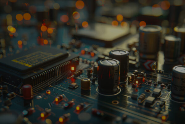
In recent years, the demand for IoT devices has increased significantly, whether it is for home appliances or for the business sector. IoT devices might seem simple for end users, but designers need to go through many complexities while designing a PCB design board.
Designers get little space to work due to the smaller size of IoT devices without compromising the functionality and speed. However, the world is on the brink of advancement for developing more versatile IoT devices. So, PCB hardware designers use multiple techniques to overcome the challenges.
In this blog, we delve into the complexities of designing a PCB design board and ways to overcome these challenges.
Size and Space Constraints
- Miniaturization Requirements
Less physical space is one of the biggest challenges for PCB designers as devices are getting smaller. They need to miniaturize PCB and optimize space as a prototype process in IoT devices. Furthermore, techniques like surface mount technology (SMT) help designers design a small PC, placing components in close proximity. This ensures the functionality of the device, irrespective of small devices.
For instance, the demand for wearables has significantly increased, which requires tiny PCBs. Its unconventional shape and size impose major restrictions on PCB design service providers, as the design needs to be minimalist. - Integration of Multiple Components
PCB design service providers need to capitalize on the design in the early stage of the PCB prototype to identify and rectify, reducing the project time and preventing the increment in production cost.
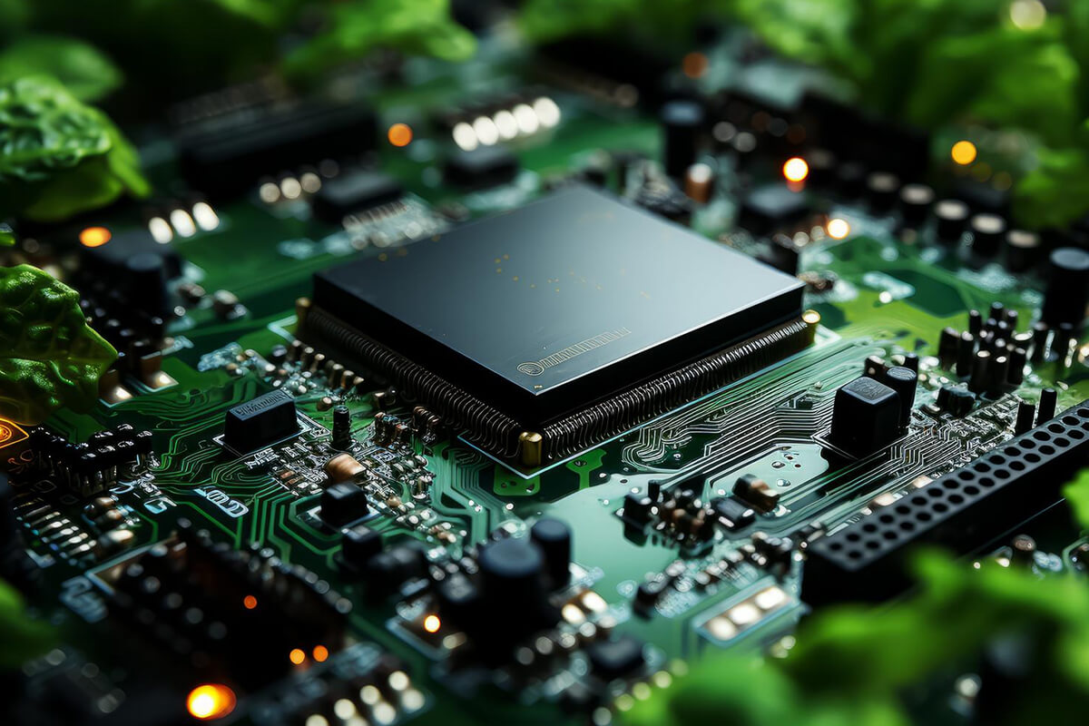
They need to ensure the integration of all electronic processes into a single board, navigating the rapid evolution of IoT devices. In addition, designers need to take seamless integration with other systems into account, along with adhering to industry standards, such as IEEE, ANSI, etc.
While integrating the electronic components, a PCB supplier needs to ensure the effective connectivity of devices by evaluating the protocols, such as Bluetooth WiFi. - Heat Dissipation
Due to compact space, managing heat dissipation can be the biggest challenge. When parts inside a device are packed closely together, they can get very hot. It can reduce performance of devices, leading to breakdown.
However, PCB can manage some heat, but too much heat can be bad. It might make parts rust or weaken, which can stop the device from working the way it should. This challenge becomes more pronounced in compact designs where there’s limited room for traditional cooling solutions like fans or heat sinks. - Signal Integrity and Noise
Signal integrity and noise are some of the most critical factors of a reduced PCB design layout. When signals travel along the PCB, Electromagnetic interference (EMI) can occur due to their proximity. This interference can cause data corruption, reduced signal quality, or incorrect functioning of electronic systems. Therefore, it’s crucial to maintain signal integrity, preventing crosstalk, electromagnetic radiation, and other interference issues. - Manufacturability
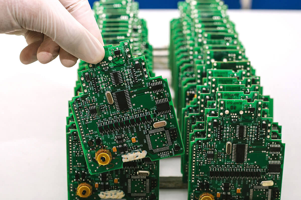
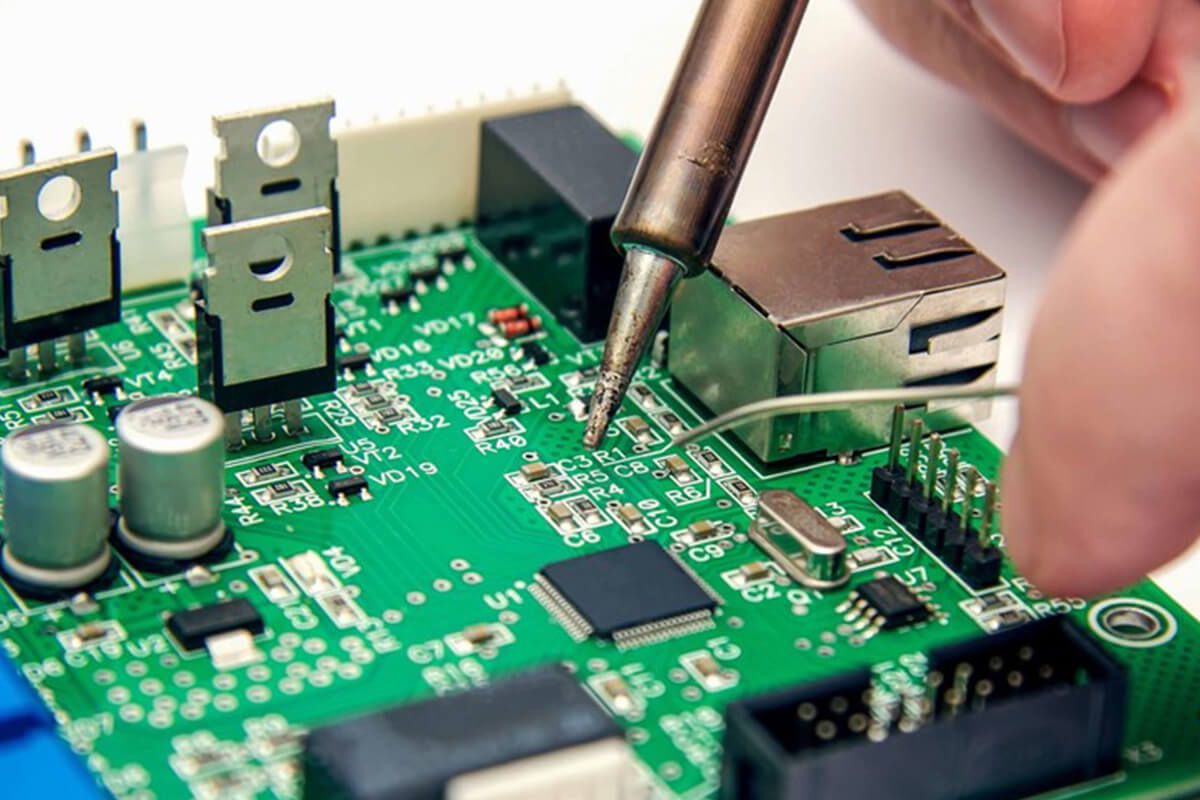
Complex layouts within confined spaces pose challenges during manufacturing. As the design becomes intricate, assembling, soldering, or testing the components can become more difficult and time-consuming. - Power Management and Energy Efficiency
A PCB supplier needs to ensure effective power management and energy conservation, reducing the negative impact of electricity-induced heat. They are required to adhere to various processes in the devices, such as energy consumption management, power regulation, and power distribution. This extends the battery life of IoT devices and fulfills the end-user requirements.
Furthermore, they ensure that unused devices will turn off, saving battery power. For this, PCB hardware designers need to put extra effort into dividing various functional blocks and allocating the power for each. They should also take the budget into consideration.
Addressing the Space and Size Constraints
- Component Selection and Integration
Component selection is one of the crucial steps in designing a PCB design board; utilize active and passive components. Active components derive power from the power source, and passive components devices don’t depend on any type of source.
In addition, choose smaller components to reduce overall footprint and incorporate multi-functional, resulting in space savings and a more streamlined design. - Advanced PCB Design Techniques
Employ HDI technology, as it aids in more complex and compact PCB layouts. This technique optimizes the use of available space, allowing more efficient routing and component placement. - Optimized Layout and Routing
Thoughtful and strategic routing minimizes signal interference and optimizes signal paths. One can use various methods to reduce crosstalk and reflection. Differential signaling reduces noise and crosstalk, as positive and negative signals are sent by parallel wire. In addition, Strategically placing components on the PCB is critical to maximize space utilization. - Thermal Management
Managing the temperature of the electronics component is critical, as heat generated by the electronics component is higher due to its compact size. Integrate heat sinks, thermal vias, and others for efficient dissipation of heat generated by components on the board. - Simulation and Testing
Simulation tools address potential signal integrity and thermal issues before the production phase. This proactive approach helps identify and rectify potential design flaws early in the process, reducing the risk of costly rework or manufacturing errors.
In addition, testing validates the design’s functionality and reliability in real-world conditions. - Collaboration with Manufacturers
Work closely with manufacturers to overcome manufacturing challenges. This can include following standard rules, such as trace width and space.
Also Know: The Role of Enterprise Hardware Solutions in Supporting Your IT Infrastructure
The Bottom Line!
In the fast-evolving landscape of IoT device development, designing PCBs within size and space constraints presents numerous challenges for hardware designers. The demand for smaller, more efficient devices continually pushes the boundaries of innovation, leading to a multitude of hurdles in the design process. That’s where Tessolve comes into the picture. We provide a PCB design board in the USA, fostering smaller IoT device development.