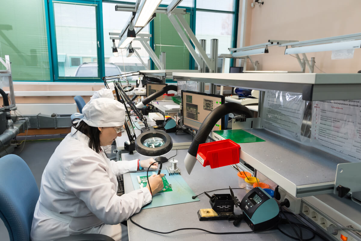
How Is Advanced IC Packaging Crucial in the Future?
If we were to summarize the future in a single term, it would be “data-centric.” Traditionally, IC Packaging Design Services providers used to design chips with all functions integrated on a single die. However, as the industry experiences the deceleration of Moore’s law, scaling monolithic ICs becomes increasingly challenging and expensive. As a result, IC vendors are now turning to “advanced semiconductor packaging” to address the growing demand for data worldwide. This shift allows them to meet the evolving data requirements more effectively and efficiently.
Data has become crucial at every level and in almost every sector. The digital world generates 4,000 TB of data every second, and it is expected that this amount will further go significantly up in the upcoming time. Data-rich applications such as AI and machine learning are the key data enablers in various applications such as 5G, data centers, and autonomous vehicles. However, a strong processor is needed to run this application, of which ICs are the foundation.
What Is Advanced Semiconductor Packaging?
Advanced semiconductor packaging involves innovative techniques and technologies to enhance the performance, functionality, and integration of integrated circuits (ICs). It goes beyond traditional methods by incorporating 3D packaging, wafer-level packaging, fan-out packaging, SiP, and MCM. These techniques enable higher integration levels, improved signal integrity, efficient thermal management, and compact form factors.
Advanced semiconductor packaging addresses the challenges of smaller device sizes, increased functionality, higher performance, and power management. It enables the development of smaller, faster, and more power-efficient electronic devices while ensuring reliability and manufacturability. This technology is crucial in meeting the evolving demands of industries like mobile devices, automotive electronics, IoT, AI, and high-performance computing.
Read More: Increased Importance of VLSI Design Ecosystem in India for Worldwide Semiconductor Industry
Future of Advanced IC Packaging
The future of advanced IC packaging holds immense potential for shaping the electronics industry. Here are some key aspects that indicate its promising trajectory:
Shrinking Form Factors and Increased Integration
Advanced IC packaging plays a pivotal role in the relentless pursuit of miniaturization and the need for compact devices. It enables the Integration of multiple components, such as microprocessors, memory modules, and sensors, into a single package. This Integration not only saves space but also enhances performance and power efficiency.
Higher Speed and Signal Integrity
Advanced IC packaging techniques like flip-chip and fan-out wafer-level packaging (FOWLP) enable shorter interconnect lengths and better signal integrity. High-speed signals can travel faster by minimizing the distance between the semiconductor die and the package, reducing latency and improving overall system performance.
Thermal Management and Power Dissipation
As electronic devices become more powerful, managing heat dissipation becomes critical. Advanced IC packaging techniques incorporate innovative thermal management solutions, such as microscale heat sinks, thermal vias, and integrated cooling technologies. These techniques enhance heat dissipation, ensuring reliable performance and preventing overheating issues.
System-Level Integration and Functionality
Advanced IC packaging enables system-level Integration, combining multiple functionalities into a single package. Through techniques like System-in-Package (SiP) and Multi-Chip Modules (MCM), diverse components can be integrated, including microcontrollers, RF modules, power management ICs, and sensors. This Integration leads to improved performance, reduced power consumption, and enhanced user experience.
High-Density Interconnects and 3D Integration
IC packaging advancements also facilitate high-density interconnects and 3D Integration, enabling more complex designs. Through technologies like Through-Silicon Vias (TSVs) and Interposer-based packaging, designers can stack multiple dies vertically, achieving greater functionality within a smaller footprint. This approach unlocks new possibilities for creating powerful and efficient devices.
Concluding Remarks
As the demand for advanced electronic devices continues to rise, the role of advanced IC packaging in hardware design and PCB solutions becomes increasingly crucial. Advanced IC packaging is shaping the future of electronics by enabling miniaturization, enhancing signal integrity, managing heat dissipation, and facilitating system-level Integration.
Tessolve, a leading provider of IC packaging design services and hardware solutions, understands the significance of advanced packaging technologies. We have designed some of the most advanced, high-performance packages on the market for our industry-leading customers. With competent Toolkits and Familiarity of delivering diverse package specifics, Tessolve ensures the best performance design is delivered to the customer.
Choose Tessolve for your advanced IC packaging needs and unlock the full potential of your electronic devices in the rapidly advancing technological landscape.
Read more: The Power of Simulations: Revolutionizing Engineering Hardware Development