How Is Advanced IC Packaging Crucial in the Future?
If we were to summarize the future in one term, it would be “data-centric.” Traditionally, IC Packaging Design Services providers designed chips with all functions integrated into a single die. However, as the industry decelerates Moore’s law, scaling monolithic ICs becomes increasingly challenging and expensive. The industry has now reached a “reticle limit” where chips physically cannot get much larger on a single die. Consequently, IC vendors are now adopting advanced semiconductor packaging to fulfill the increasing global demand for data. This transition enables them to address evolving data requirements more efficiently.
Data has become crucial at every level and in almost every sector. Data-rich applications such as Generative AI and Large Language Models (LLMs) are key data enablers across high-speed networking, data centers, and autonomous vehicles. However, a powerful processor is needed to run these applications, and ICs are the foundation. Advanced packaging now serves as the “bridge” that bypasses the memory wall, allowing High-Bandwidth Memory (HBM) to be placed in the same package as the processor for near-instantaneous data access.
What Is Advanced Semiconductor Packaging?
Advanced semiconductor packaging involves innovative techniques and technologies to enhance the performance, functionality, and integration of integrated circuits (ICs). It goes beyond traditional methods by incorporating 3D packaging, wafer-level packaging, fan-out packaging, SiP, and MCM. These techniques enable higher integration levels, improved signal integrity, efficient thermal management, and compact form factors.
Advanced semiconductor packaging addresses the challenges of smaller device sizes, increased functionality, higher performance, and power management. It enables the development of smaller, faster, and more power-efficient electronic devices while ensuring reliability and manufacturability. This technology is crucial in meeting the evolving demands of industries like mobile devices, automotive electronics, IoT, AI, and high-performance computing.
Read More: Increased Importance of VLSI Design Ecosystem in India for Worldwide Semiconductor Industry
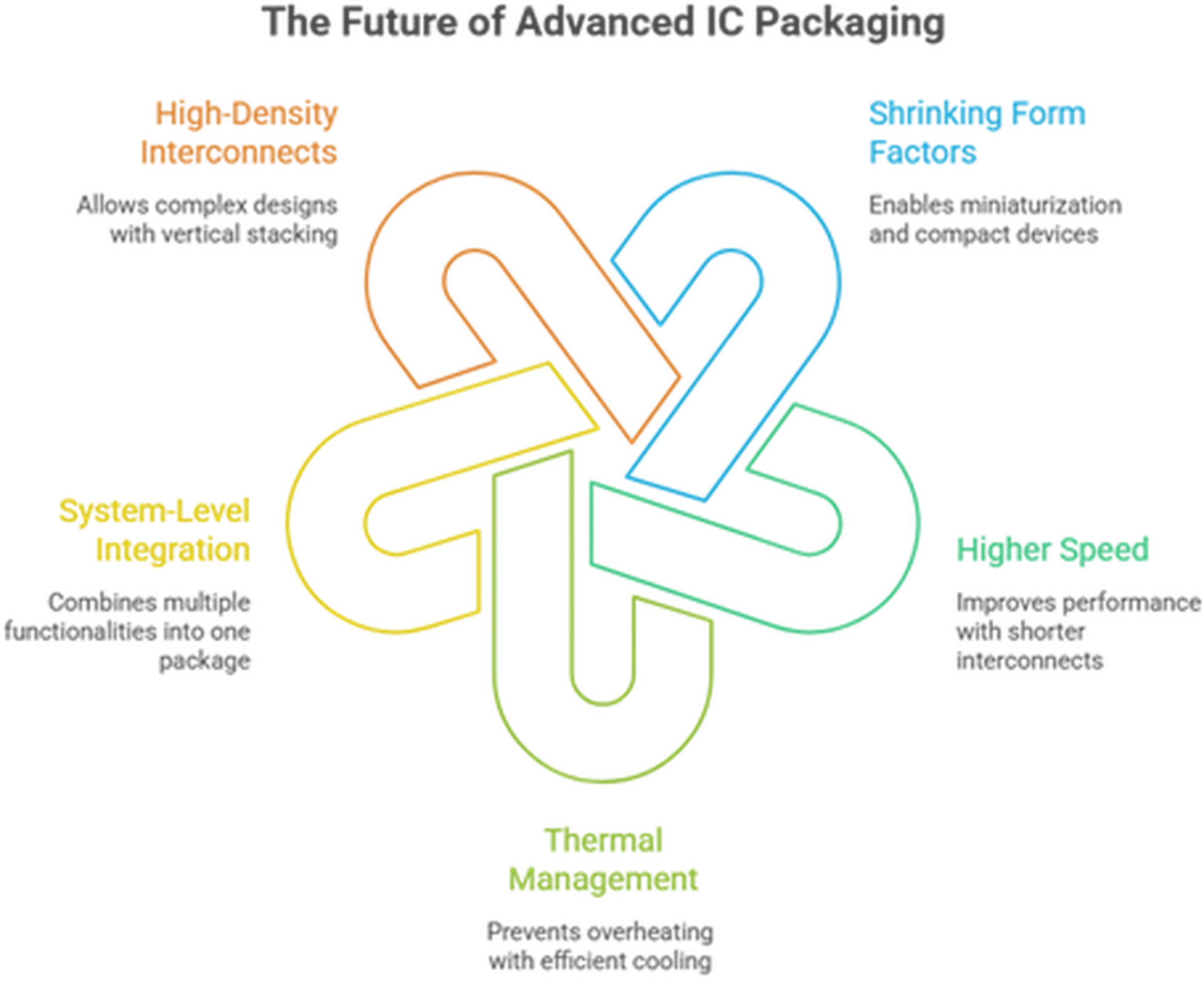
The future of advanced IC packaging holds immense potential for shaping the electronics industry. Here are some key aspects that indicate its promising trajectory:
Shrinking Form Factors and Increased Integration
Advanced IC packaging plays a pivotal role in the relentless pursuit of miniaturization and the need for compact devices. The shift from monolithic designs to heterogeneous integration allows designers to use the most advanced process nodes (like 3nm or 2nm) for logic while using more cost-effective nodes for I/O and analog components. This Integration not only saves space but also enhances performance and power efficiency.
Higher Speed and Signal Integrity
Advanced IC packaging techniques like Fan-Out Wafer-Level Packaging (FOWLP) and Co-Packaged Optics (CPO) enable shorter interconnect lengths and better signal integrity. By integrating optical engines directly within the package, signals can be converted to light immediately, virtually eliminating the electrical losses associated with traditional copper traces over long distances. This reduces latency and improves overall system performance.
Thermal Management and Power Dissipation
As electronic devices become more powerful, managing heat dissipation becomes critical. Advanced IC packaging techniques incorporate innovative thermal management solutions, such as microscale heat sinks, thermal vias, and integrated cooling technologies. These techniques enhance heat dissipation, ensuring reliable performance and preventing overheating issues.
System-Level Integration and Functionality
Advanced IC packaging enables system-level Integration, combining multiple functionalities into a single package. Through techniques like System-in-Package (SiP) and Multi-Chip Modules (MCM), diverse components can be integrated, including microcontrollers, RF modules, power management ICs, and sensors. In modern automotive and industrial applications, this allows for “Sensor-to-Cloud” integration where sensing and AI processing happen within the same physical package.
High-Density Interconnects and 3D Integration
IC packaging advancements also facilitate high-density interconnects and 3D Integration, enabling more complex designs. Through technologies like Through-Silicon Vias (TSVs) and Interposer-based packaging, designers can stack multiple dies vertically, achieving greater functionality within a smaller footprint. This approach unlocks new possibilities for creating powerful and efficient devices.
Concluding Remarks
As the demand for advanced electronic devices continues to rise, the role of advanced IC packaging in hardware design and PCB solutions becomes increasingly crucial. Advanced IC packaging is shaping the future of electronics by enabling miniaturization, enhancing signal integrity, managing heat dissipation, and facilitating system-level Integration.
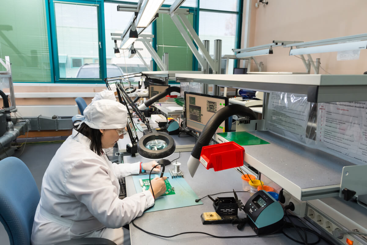
Tessolve, a leading provider of IC packaging design services and hardware solutions, understands the significance of advanced packaging technologies. Our expertise in Silicon Lifecycle Management (SLM) and complex 3D assembly ensures that your hardware is ready for the next generation of data-centric computing. We have designed some of the most advanced, high-performance packages on the market for our industry-leading customers. With competent toolkits and familiarity with delivering diverse package specifics, Tessolve ensures the best performance design is delivered to the customer.
Frequently Asked Questions
1. Why is advanced packaging replacing monolithic chip designs?
As silicon scaling becomes too expensive, advanced packaging allows “chiplets” from different nodes to work together, improving yield and lowering costs.
2. What are the top solutions for advanced packaging in IC manufacturing?
Leading solutions include 2.5D/3D-IC stacking, Fan-Out Wafer-Level Packaging (FOWLP), and System-in-Package (SiP). These utilize silicon interposers and through-silicon vias (TSVs) to integrate high-bandwidth memory and heterogeneous chiplets effectively.
3. What are the different stages of IC design, and how can IC consultancy assist at each stage?
Stages include specification, architecture, RTL design, physical layout, and verification. Consultancies provide specialized expertise in power optimization, timing closure, and “Design for Manufacturability” (DFM) to accelerate production timelines.
4. What does “advanced packaging” mean in the context of semiconductors?
It refers to aggregation and interconnection techniques that merge multiple dies into a single high-performance package. This approach bypasses traditional monolithic limits, enhancing speed, density, and thermal efficiency.
5. How does Co-Packaged Optics (CPO) impact data centers?
CPO moves optical connections closer to the processor, reducing power consumption and allowing for the massive bandwidth required by AI workloads.


