The semiconductor industry is undergoing rapid advancements characterized by increasing complexity and miniaturization. Staying at the forefront of this evolution necessitates forging alliances with a new generation of collaborators. As chip designs approach the atomic scale (TERA-scale), it is imperative to engage individuals equipped to anticipate and resolve challenges at this pioneering frontier while remaining attuned to ongoing innovation.
Tessolve is a prominent worldwide supplier of engineering services to the semiconductor sector, and this is where top semiconductor companies turn to them. Tessolve offers a comprehensive range of solutions covering the entire product lifecycle, from semiconductor design to semiconductor testing and production enablement. These solutions facilitate the development of advanced semiconductors for the future.
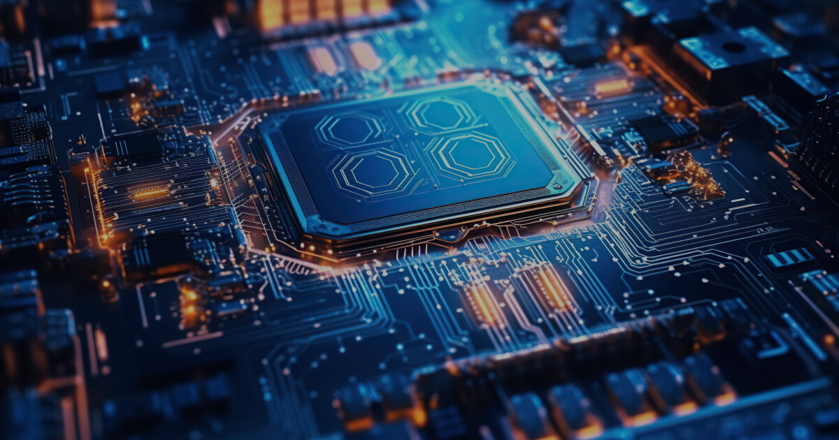
The TERA-Scale Challenge
As we approach the TERA-scale, the challenges become more pronounced. Moore’s Law, a guiding principle for the semiconductor industry for over 50 years, is reaching its physical limits. Downsizing is becoming increasingly difficult and costly, with issues like leakage currents, quantum tunneling effects, and thermal management problems posing significant obstacles.
Tessolve’s Expertise Across the Semiconductor Life cycle
Tessolve gives businesses leverage throughout the chip-making process. From the initial design (architecture, logic, physical) by a team with extensive semiconductor design company knowledge to crucial semiconductor testing company like functional and logic testing to guarantee chip health before production, their skilled engineers provide a full range of services. Semiconductor process engineers assist clients with efficient manufacturing, and embedded systems development guarantees smooth hardware-software integration for optimal performance. Tessolve is unique in that it has experience in every step.
Tessolve’s Enabling Solutions
Tessolve uses a unique blend of state-of-the-art technology, industry knowledge, and a worldwide delivery strategy to meet these issues. Here’s a closer look at how they make it possible for the upcoming semiconductor generation:
- Advanced Design Services: Tessolve’s team of experienced semiconductor design company engineers provides a comprehensive set of design services, including RTL coding, physical design, verification, and IP integration. They use cutting-edge design tools and techniques to produce optimized designs that satisfy the demanding PPA (performance, power, and area) specifications of TERA-scale chips.
- Skilled Silicon Validation: Ensuring chip operation requires both functional and physical verification. Tessolve’s verification specialists find and fix design flaws early in the development cycle with the use of sophisticated simulation tools and techniques. This guarantees the first-time silicon success of intricate TERA-scale designs while simultaneously cutting down on development time and expenses.
- Next-Gen Test Engineering: As chip complexity rises, conventional test techniques are no longer sufficient. Tessolve provides an extensive range of next-generation test solutions, such as enhanced test pattern development, DFT (Design for Test) optimization, and embedded testing. With the help of these technologies, semiconductor testing businesses may successfully test and guarantee the quality and dependability of TERA-scale devices.
- Manufacturing Know-How: Getting from design to production can be challenging. The manufacturing engineers at Tessolve fill in the gaps with their knowledge of subjects like process engineering and design for manufacturability (DFM). They work together with fabs to guarantee high yields and efficient manufacturing of TERA-scale designs.
- Global Delivery methodology: By utilizing this methodology, Tessolve can access a global pool of highly qualified engineers. This guarantees that clients, wherever they may be, will always have access to the right talent at the right moment. Their economic strategy also aids in reducing time-to-market for next-generation semiconductors and optimizing research costs.
Tessolve: A Partner for the Future
TERA-scale semiconductor development faces obstacles. However, by working with Tessolve, businesses may overcome these obstacles and become pioneers in the design and production of the upcoming generation of chips. Due to their dedication to innovation, extensive industry knowledge, and global reach, any business creating cutting-edge semiconductor solutions would find Tessolve to be an excellent resource.
A top semiconductor company may save development costs, accelerate time to market, and produce next-generation devices that push the envelope of what is feasible by utilizing Tessolve’s expertise. Tessolve continues to be a reliable partner in the semiconductor industry’s unrelenting march towards complexity and downsizing, facilitating the development of the chips that will drive the future.
A Commitment to Quality and Innovation
Tessolve’s success is primarily due to their unwavering dedication to quality. They follow strict guidelines for quality throughout the entire process of design and production. By doing this, they guarantee that their customers will receive dependable and efficient semiconductor products. Tessolve also makes significant investments in R&D to stay on the cutting edge. They are constantly investigating new technologies and approaches to deal with the changing difficulties facing the semiconductor sector.
Efficient RTL Design Strategies for
VLSI Integration
Let’s Conclude
Tessolve’s steadfast commitment to excellence, ingenuity, and a diverse array of services offers semiconductor firms the confidence that they can surmount challenges and develop pioneering products with a far-reaching impact on the industry’s journey toward TERA-scale integration.


