The rollout of 5G technology has redefined the connectivity landscape, ushering in unprecedented speeds, reduced latency, and enhanced capacity. There are unique challenges and opportunities for PCB design engineers tasked with supporting this next-generation network. To successfully design PCBs for 5G applications, engineers must address several key considerations—from high-frequency signal integrity to thermal management. This blog explores the critical aspects of PCB hardware design for 5G and highlights best practices for engineers and organizations seeking effective PCB solutions.
The Role of PCBs in the 5G Revolution
Printed Circuit Boards (PCBs) form the backbone of modern electronics, and their role in the 5G revolution is pivotal. As devices and infrastructure become more advanced, PCBs must meet the demanding requirements of higher frequencies, faster data rates, and compact designs.
Engineers must embrace innovative PCB hardware design techniques to ensure devices function reliably in diverse 5G applications. From consumer electronics to industrial IoT devices, every component relies on a well-optimized PCB. By focusing on robust PCB solutions, designers can contribute to the seamless deployment of 5G technologies across industries.
Essential Guidelines for Engineers and Organizations
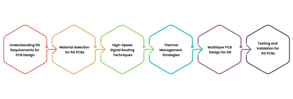
To address the complexities of 5G design, engineers and organizations must adopt a comprehensive approach that encompasses all critical aspects of PCB development. Below are best practices categorized under specific focus areas:
1. Understanding 5G Requirements for PCB Design
5G networks demand higher frequency ranges, with mmWave bands extending beyond 24 GHz. These high frequencies enable faster data transmission and lower latency but introduce significant challenges for PCB hardware design due to factors like signal attenuation and electromagnetic interference (EMI). Engineers must account for the following:
- Signal Integrity: Maintaining signal integrity at high frequencies requires meticulous trace design, strict impedance control, and precise material selection. Even minor mismatches in impedance can lead to signal distortion or significant signal loss, impacting overall performance.
- Thermal Management: High-power 5G components, such as power amplifiers and transceivers, generate substantial heat. Advanced thermal dissipation mechanisms, including thermal vias, heat sinks, and optimized copper planes, are essential for ensuring reliable operation.
- Compact Design: The growing demand for smaller and more portable 5G devices necessitates highly dense, multilayer PCBs. These designs must accommodate high-speed signals, power delivery, and component placement without compromising performance.
- Electromagnetic Compatibility (EMC): Higher operating frequencies increase susceptibility to EMI, requiring engineers to employ robust shielding techniques, proper grounding, and optimized layout strategies to minimize interference.
2. Material Selection for 5G PCBs
Choosing the right materials is a cornerstone of successful PCB design for 5G. Materials must exhibit low dielectric constant (Dk) and low loss tangent (δ), which are essential for minimizing signal degradation at high frequencies. Key material options include:
- PTFE (Polytetrafluoroethylene): Renowned for its exceptional electrical properties, PTFE is a preferred choice for mmWave applications. However, it requires specialized manufacturing processes, which can increase costs.
- Rogers Laminates: High-frequency laminates, such as the Rogers RO3000 and RO4000 series, offer a balance of superior performance and cost-efficiency, making them widely used in 5G PCB designs.
- FR4 with High-Speed Additives: While standard FR4 is inadequate for 5G applications, advanced variants enhanced with high-speed additives can support lower-frequency 5G designs, providing a cost-effective alternative for specific use cases.
Key Material Properties to Consider:
- Dielectric Constant (Dk): Ensures consistent signal propagation across PCB traces.
- Loss Tangent (δ): Minimizes signal attenuation, particularly at mmWave frequencies.
- Thermal Conductivity: Supports effective heat dissipation in high-power designs.
- Coefficient of Thermal Expansion (CTE): Ensures mechanical stability during thermal cycling to avoid material deformation or failure.
Collaborating with a trusted PCB design service can help organizations navigate these material selection complexities and ensure optimal performance for 5G devices.
3. High-Speed Signal Routing Techniques
Routing high-frequency signals on a PCB requires precision to maintain signal integrity and prevent degradation. Best practices include:
- Controlled Impedance: Ensure consistent trace impedance by maintaining uniform trace width, spacing, and stack-up. This reduces signal reflections and improves signal quality.
- Differential Pair Routing: Use differential pairs for high-speed signals, with equal trace lengths and precise spacing, to maintain signal balance and minimize crosstalk.
- Minimizing Stub Lengths: Shorten stub lengths to prevent signal reflections and reduce impedance mismatches, which can impact signal integrity.
- Ground Planes: Employ continuous ground planes under high-speed traces to reduce noise, improve EMI performance, and enhance signal return paths.
A skilled PCB design engineer integrates these techniques seamlessly into the design to meet stringent 5G performance requirements.
4. Thermal Management Strategies
Effective thermal management is critical for 5G PCBs, as high-speed components often operate at elevated power levels, generating significant heat. Recommended strategies include:
- Thermal Vias: Place thermal vias under heat-generating components to transfer heat to other layers of the PCB, improving overall heat dissipation.
- Heat Sinks and Spreaders: Attach heat sinks or spreaders to components to redirect heat away efficiently, extending the device’s operational lifespan.
- Copper Planes: Use thicker copper planes to enhance the PCB’s thermal conductivity and distribute heat more effectively.
- Simulation Tools: Leverage advanced thermal simulation software to model heat dissipation, identify hotspots, and optimize cooling strategies.
Collaborating with a professional PCB design service ensures that these thermal management techniques are implemented effectively for robust and reliable operation.
Thermal Management Strategies for High-Performance PCBs
5. Multilayer PCB Design for 5G
5G devices often require multilayer PCBs to accommodate complex routing, high-speed signal paths, and power distribution networks (PDNs). Key considerations for multilayer designs include:
- Stack-Up Design: Define an optimized layer stack-up to reduce signal crosstalk and maintain signal integrity across high-frequency traces.
- Power Distribution Network (PDN): Design a robust PDN with sufficient decoupling capacitors to ensure stable power delivery under varying loads.
- Via Placement: Use advanced technologies, such as micro vias and buried vias, to connect layers effectively while minimizing parasitic inductance and resistance.
An experienced PCB design engineer carefully balances these factors to deliver multilayer designs that combine high performance, manufacturability, and cost-efficiency.
6. Testing and Validation for 5G PCBs
Thorough testing and validation are essential to ensure that 5G PCBs meet the demanding performance and reliability standards required for deployment. Common techniques include:
- Signal Integrity Testing: Use vector network analyzers (VNAs) to measure S-parameters, ensuring that signal integrity is maintained across the operating frequency range.
- Thermal Analysis: Perform thermal cycling tests to evaluate heat dissipation, material stability, and overall thermal performance under varying conditions.
- EMI Testing: Conduct comprehensive electromagnetic interference tests to ensure compliance with industry standards and regulatory requirements.
- Prototyping: Develop and test functional prototypes to validate the design before moving into full-scale production, minimizing risks and accelerating time-to-market.
By leveraging comprehensive PCB solutions, organizations can streamline testing processes, ensure compliance with 5G standards, and gain a competitive edge in the fast-evolving 5G landscape.
Streamlining 5G Product Development with Tessolve’s NPI Expertise
New Product Introduction (NPI) is a critical phase in 5G product development, ensuring smooth transitions from design to manufacturing. Tessolve’s NPI services stand out by offering a comprehensive approach that reduces time-to-market while maintaining high-quality standards. From initial prototyping to volume production, Tessolve’s expertise spans design validation, test development, and supply chain optimization.
A key element of Tessolve’s NPI process is its focus on Design for Manufacturability (DFM) and Design for Testability (DFT). By addressing potential manufacturing and testing challenges early in the design phase, Tessolve helps clients mitigate risks and improve production efficiency. Their advanced facilities and experienced teams also enable quick turnaround times, which is essential for the fast-paced 5G market.
Collaborating with Tessolve’s NPI services ensures that businesses can navigate the complexities of 5G product development with confidence, delivering reliable and innovative solutions to market faster.
Streamlining 5G Product Development with Tessolve’s NPI Expertise
How Will 5G Transform the Aviation Industry?
The aviation industry is on the cusp of a major transformation driven by the capabilities of 5G networks. Tessolve highlights several ways 5G will revolutionize aviation, from enhanced communication systems to improved passenger experiences.
5G enables ultra-reliable, low-latency communication, which is critical for air traffic management and in-flight connectivity. Pilots, air traffic controllers, and ground staff can benefit from seamless communication, improving safety and operational efficiency. Additionally, 5G’s high bandwidth supports real-time data transfer, enabling predictive maintenance and reducing downtime.
Passengers, too, stand to gain significantly from 5G’s advancements. High-speed in-flight internet and personalized entertainment systems will redefine the travel experience. Airlines can also leverage 5G to enhance customer service through AI-driven applications and real-time updates.
As Tessolve’s insights reveal, the integration of 5G in aviation is poised to create smarter, safer, and more connected air travel ecosystems.
How Will 5G Transform the Aviation Industry?
The Future of Connectivity: Exploring 5G Networks
The future of connectivity lies in the potential of 5G networks to reshape industries and redefine communication. Tessolve’s analysis underscores the transformative impact of 5G, highlighting its role in enabling technologies such as the Internet of Things (IoT), autonomous vehicles, and smart cities.
5G’s ability to support massive machine-type communication (mMTC) and ultra-reliable low-latency communication (URLLC) makes it a cornerstone for technological advancements. Industries like healthcare, manufacturing, and transportation are leveraging 5G to drive efficiency and innovation. For instance, IoT devices connected through 5G can streamline operations and provide real-time analytics, while autonomous vehicles benefit from near-instantaneous data exchange.
Tessolve’s expertise in 5G infrastructure development ensures that businesses can harness these capabilities effectively. Their end-to-end solutions support the design, testing, and deployment of 5G networks, enabling seamless integration with emerging technologies.
Partnering with Tessolve for Your 5G PCB Needs
As a global leader in semiconductor and PCB design service, Tessolve offers end-to-end solutions for 5G hardware design. With expertise in high-speed PCB layout, signal integrity analysis, and thermal management, Tessolve empowers businesses to overcome 5G challenges. Their comprehensive portfolio includes PCB hardware design, prototyping, and testing services tailored to next-generation connectivity.
Tessolve’s team of experienced PCB design engineers collaborates closely with clients to deliver optimized PCB solutions that meet stringent 5G performance requirements. Whether you need assistance with material selection, multilayer design, or validation, Tessolve provides the expertise and resources to ensure success. Learn more about their cutting-edge offerings at Tessolve.
Let’s Conclude
Designing PCBs for 5G connectivity is a complex yet rewarding endeavor. From material selection to high-speed routing and thermal management, every aspect of PCB hardware design plays a crucial role in achieving optimal performance. By adhering to best practices and leveraging professional PCB design services, engineers can overcome the challenges posed by 5G technology. Partnering with trusted providers like Tessolve ensures access to the expertise and tools necessary for success, enabling organizations to stay ahead in the race for next-generation connectivity.