
The demand for sleeker, more compact, and high-performing electronic devices continues to grow across industries, from smartphones and wearables to automotive and aerospace systems. To meet this demand, engineers increasingly turn to 3D multilayer PCBs, which allow more components to be packed into a smaller area while maintaining robust electrical performance.
However, designing compact PCBs is not just about fitting more traces into a limited space. The challenge lies in reducing the footprint without compromising signal integrity, power delivery, or manufacturability. This blog explores the most effective layout techniques that every PCB design engineer can leverage to achieve compact designs while ensuring reliable performance.
Why Footprint Reduction Matters in Modern PCB Design
Today’s electronic products are expected to deliver higher performance in smaller, sleeker enclosures. This means every square millimeter of a PCB design board must be optimized. Compact layouts enable smaller device form factors, reduce material costs, and support higher functionality in portable applications. However, footprint reduction must be balanced with thermal reliability, manufacturability, and electrical performance. Without careful planning, a smaller board can result in poor signal quality, power noise, or premature failures. This is why innovative layout techniques are vital for any PCB design service targeting high-density, reliable designs.
Layout Techniques to Reduce Footprint
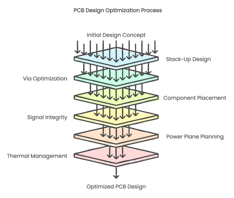
1. Start with a Thoughtful Stack-Up Design
A well-structured stack-up is the backbone of a 3D multilayer PCB design board. By carefully defining signal, ground, and power planes, you can optimize both space usage and signal performance.
- Place ground planes adjacent to high-speed signal layers to maintain controlled impedance.
- Use thin dielectrics and high-performance laminates to reduce crosstalk and insertion loss.
- Leverage HDI techniques like sequential lamination to add routing density without increasing board size.
This step ensures you can reduce board area while still supporting high-speed signals and minimizing electromagnetic interference.
2. Optimize Via Usage for Vertical Routing
Instead of relying on traditional through-hole vias, use:
- Microvias for inter-layer connections.
- Blind and buried vias to ease outer-layer congestion.
- Via-in-pad for dense BGA breakout.
These techniques allow a PCB design engineer to utilize vertical routing, freeing up lateral space for additional signals.
3. Effective Component Placement
Component placement is both art and science. High-pin-count devices like BGAs should sit centrally to reduce routing lengths, while connectors belong at the edges for accessibility. Grouping passives close to their respective IC pins reduces clutter. By also choosing smaller or stacked packages, a PCB design service can save valuable space without affecting electrical efficiency.
4. Maintain Signal Integrity with Routing Discipline
To preserve performance in compact boards, follow disciplined routing methods:
- Maintain consistent trace width and spacing for controlled impedance.
- Match trace lengths in differential pairs.
- Back-drill vias to eliminate stubs.
- Use ground stitching to shield sensitive nets.
These steps prevent reflections, crosstalk, and EMI issues as density increases.
5. Power Plane Planning for Compact Designs
Shrinking a PCB does not reduce the demand for stable power. Splitting power planes across layers while stitching ground vias at strategic points helps maintain return paths. Decoupling capacitors should be placed as close as possible to IC pins, and thicker copper pours should be used for high-current sections. This ensures the compact PCB design board supports clean and reliable power delivery.
6. Balance Density with Thermal Management
A compact multilayer board often generates concentrated heat. Techniques like thermal vias beneath ICs, copper pours for heat spreading, and thermally conductive laminates are crucial. A PCB design engineer must integrate thermal relief strategies into the layout to avoid hot spots and ensure long-term device reliability.
7. Collaborate Early with Manufacturing Partners
Reducing footprint is not only an engineering challenge but also a manufacturing one. Advanced multilayer layouts often involve sequential lamination, filled microvias, and fine-line etching. Working closely with your PCB fabricator early in the process ensures:
- Feasible aspect ratios for vias.
- Manufacturable annular rings and pad sizes.
- Reduced risk of costly re-spins.
Collaboration streamlines the PCB design service while ensuring your layout translates smoothly from design to production.
8. Use Simulation and Prototyping to Validate Designs
Simulation is indispensable for compact boards. By running SI/PI simulations, designers catch issues like reflections, voltage drops, or resonance before fabrication. Building prototypes and then validating these results under real-world conditions. This iterative approach ensures that even the smallest PCB design board meets performance goals.
SI/PI Co-Simulation in High-Speed PCB Design: Reducing Post-Fabrication Surprises
Additional Considerations for Compact PCB Layouts
When working on footprint reduction in PCB design boards, keep these additional factors in mind to avoid last-minute design challenges:
- Design Rule Checks (DRC): Regularly run DRCs during layout to catch clearance and spacing issues early.
- Testability: Ensure access to test points even in compact layouts to avoid costly debugging challenges later.
- Material Selection: Choose laminates with low-loss properties for high-speed designs and better thermal stability.
- Signal Isolation: Separate analog, digital, and RF sections to minimize interference in small board areas.
- Mechanical Constraints: Factor in enclosure dimensions, connector placement, and mounting holes before finalizing the footprint.
- Cost vs. Complexity: Balance advanced HDI techniques with fabrication costs to stay within budget.
- Scalability: Design with potential product upgrades in mind, leaving space or layers for future additions.
These considerations help a PCB design engineer achieve a design that is compact, manufacturable, and scalable.
Why Tessolve is Your Trusted Partner for Multilayer PCB Design
Tessolve helps customers bring compact, high-performance products to life with our advanced PCB design service. Our team of skilled PCB design engineers specializes in creating optimized layouts for HDI, sequential lamination, and microvia-based designs. We deliver end-to-end solutions, from schematic capture and stack-up design to routing, simulation, and prototyping.
What makes Tessolve unique is our integration of design and validation. Beyond delivering a reliable PCB design, we operate in-house labs equipped for signal integrity testing, thermal analysis, and compliance verification. This ensures your design is not only space-efficient but also robust and production-ready. With Tessolve, you gain a partner that reduces design iterations, shortens time-to-market, and guarantees dependable PCB performance.