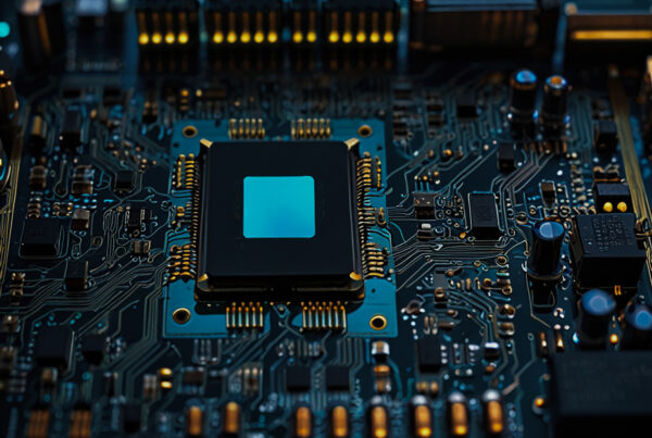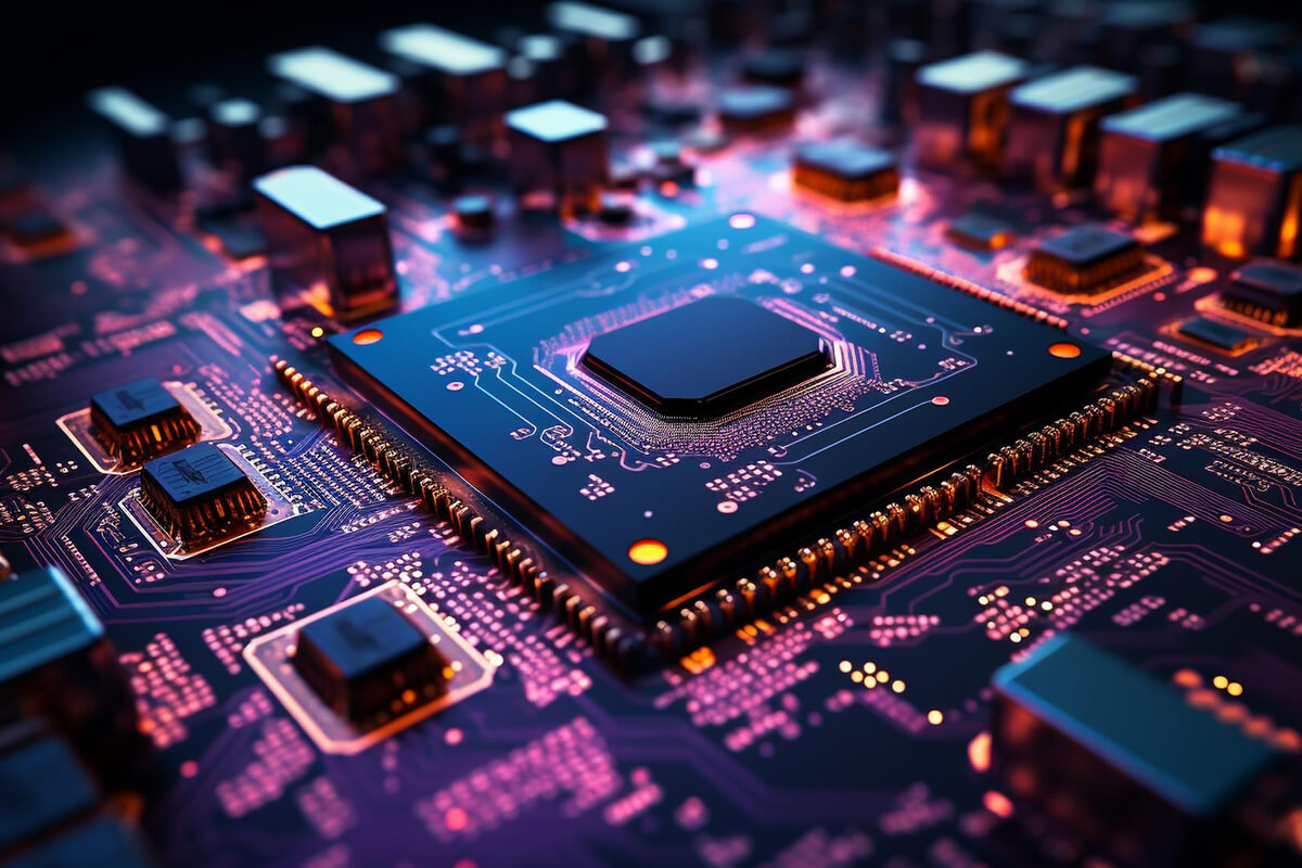
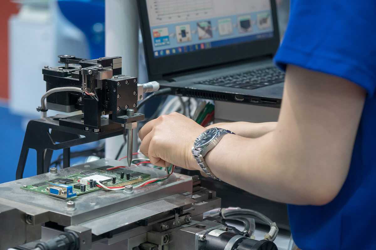
Semiconductor test engineering is an essential part of manufacturing, especially as integrated circuit (IC) designs become more complex and time-to-market pressures increase. As more transistors continue to be fabricated on a single integrated circuit, it is necessary to ensure that the processing defect is not impaired.
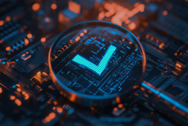
Test engineering plays a crucial role in the semiconductor industry, contributing to developing and producing high-quality semiconductor devices. Its primary focus is to ensure that semiconductor chips meet specified performance, reliability, and quality standards before they are shipped to customers.
Significance of Test Engineering in the Semiconductor Industry
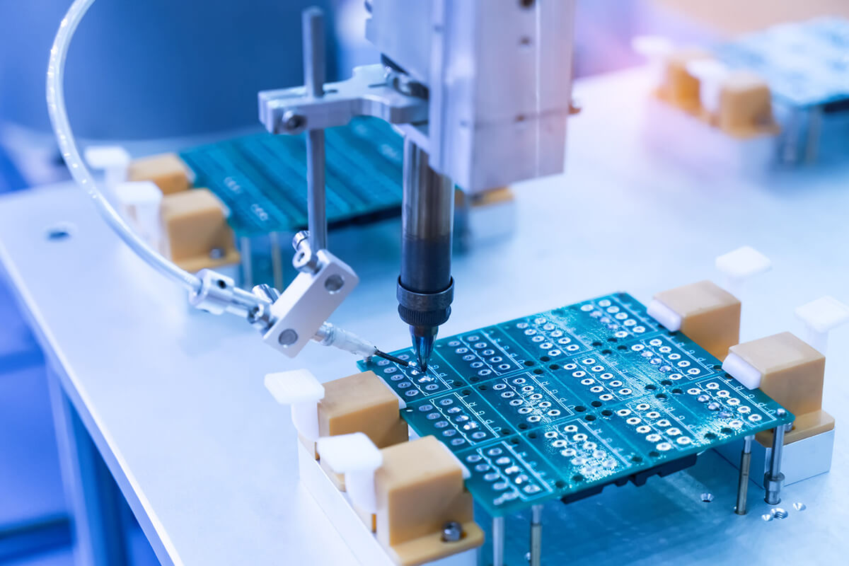
- In Test engineering, the functionality and performance of semiconductor devices are accessed through the development of test programs and methodologies. Test engineers design various tests and scripts to validate the chip features and functions.
- Extensive testing methodologies are used to identify and address defects, manufacturing variations, and other issues that potentially impact the chip’s performance. Test engineers select and maintain specialized test equipment, Automated Test Equipment (ATE), Oscilloscope, and other testing equipment.
- Test engineers conduct reliability tests, such as HighTemperature Operating Life( HTOL), ElectroStatic Discharge (ESD), Latch-Up (LU), Temperature Cycling (TC), Thermal aging, and accelerated life testing, to assess how semiconductors perform under extreme conditions and over time.
Latest Testing Equipment for Semiconductor
Decapsulation
It refers to removing the protective outer layers or encapsulation materials from a semiconductor device to access and analyze the internal components. This process is often necessary to understand the causes of semiconductor device defects, failures, or performance issues. It is used to gain access to the underlying semiconductor die or integrated circuit for various purposes, such as failure analysis, reverse engineering, design improvements and quality control.
Methods to perform decapsulation:-
Chemical Etching:
It is a standard method for decapsulation. It involves immersing the packaged device in a chemical solution that selectively dissolves the encapsulation material while leaving the silicon die or IC intact.
Laser Decapsulation:
Laser ablation can be used to remove encapsulation materials selectively. It is a precise and controlled method that minimizes the risk of damage to the underlying semiconductor components.
Failure Analysis:
Decapsulation is a crucial step in the failure analysis process. It helps investigators determine whether a device failed due to internal defects, such as wire bond failures, delamination, contamination, or if external factors were responsible.
Optical Microscopy:
Optical microscopy plays a significant role in semiconductor testing and analysis. It is a versatile tool that allows engineers and researchers to visually inspect semiconductor devices, evaluate their quality, and identify various issues and anomalies. Let’s see how it is used
Visual Inspection:
Optical microscopes are used for routine visual inspection of semiconductor wafers, packaged devices, and integrated circuits. Engineers and technicians can examine the devices for visible defects, such as cracks, scratches, contamination, or bond wire issues. Visual inspection is essential to quality control and process monitoring in semiconductor manufacturing.
Defect Localization:
When a semiconductor device fails or exhibits performance issues, optical microscopy can help localize and identify the specific area or component responsible for the problem. By zooming in on the device, analysts can pinpoint defects affecting device functionality, such as shorts, opens, or delaminations.
Wafer Mapping:
Optical microscopes can capture images of entire semiconductor wafers, allowing for wafer mapping and defect localization. This is crucial for identifying areas of concern and optimizing the manufacturing process.
Post-Failure Analysis:
After a semiconductor device has failed, optical microscopy can be used in conjunction with other techniques, such as scanning electron microscopy (SEM) or transmission electron microscopy (TEM), to investigate the root cause of the failure.
Do Test Packages Have Any Role to Play in Semiconductor Testing
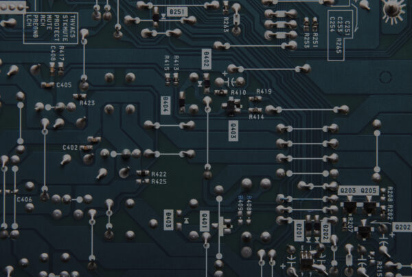
Test packages, also known as test fixtures or sockets, play a major role in test engineering and management semiconductor testing, especially for packaged integrated testing (ICs). These packages are designed to facilitate the electrical testing of semiconductor devices and ensure they function correctly. Below are the key points that illustrate the role of test packages in semiconductor testing.
Physical Protection: Test packages serve as protective enclosures for semiconductor devices during test engineering. They shield the device from physical damage, electrostatic discharge (ESD), and contamination. This is especially critical because semiconductor devices are often sensitive to external factors.
Physical Protection:
Test packages serve as protective enclosures for semiconductor devices during test engineering. They shield the device from physical damage, electrostatic discharge (ESD), and contamination. This is especially critical because semiconductor devices are often sensitive to external factors.
Thermal Management:
Some semiconductor devices generate heat during testing, affecting their performance or reliability. Test packages may incorporate features for thermal management, such as heat sinks or cooling systems, to maintain the device’s temperature within acceptable limits.
Signal Integrity:
Maintaining signal integrity is crucial in semiconductor testing. Test packages are engineered to minimize signal losses, reflections, and noise, ensuring test signals accurately represent the device’s behavior.
Understanding the Difference: Hardware Design vs. PCB Design
Avail the Testing Proficiency Within a Robust Test Setup: Choose Tessolve
We are renowned for our Engineering Testing Services and help semiconductor product companies in Semiconductor IC Design, Test and Product Engineering, PCB Design, Failure Analysis, and Systems design. We provide expensive equipment, like optical microscopy, which is expensive equipment to analyze chip layouts, bonding arrangements, etc. Moreover, we offer
Characterization Lab is a unique facility in India to perform complete Electrical Level characterization of Silicon Devices and is aided by the Government Of India.
We are a one-stop place for Semiconductor companies looking for Test and product engineering solutions. With us, you can perform Testing, Debugging, and Characterizing the devices using advanced technologies cost-effectively and quickly.