Can you imagine a world without technology, where there are no computers, mobile phones, televisions, automobiles, AC, or airplanes?
Without a proper PCB layout, a device cannot function properly. Creating a PCB design board is the same as completing a complex, multi-dimensional engineering puzzle wherein a team of engineers spends weeks or months creating the patterns. Developing a PCB layout is not a cakewalk, but anyone with proper guidance and knowledge can also do it. If you are looking for a comprehensive PCB design service, understanding these concepts is key.
With this article, we’ll help you understand the essential concepts and cutting-edge considerations that define the modern PCB layout design process.
What is a PCB Layout?
A layout is characterized by the pattern of laying out parts of a particular item or arranging them meaningfully. In the same way, the PCB layout indicates several processes that are required in designing the printed circuit board. It involves creating traces, mounting holes, cutouts, putting labels, specifying locations of various components, etc.
A significant concept in PCB design is wire routing, which is one of the most daunting tasks. Routing is the subsequent step once the placement is done. In the placement part, engineers determine the location of different components on the PCB. In routing, wires are added to connect the components as per the design rules.
PCB designing is done manually & automatically. However, to eliminate human errors these days, the designing is done using various PCB designing software. The modern approach is to use Constraint-Driven Design, where high-speed rules are defined upfront. This saves time as well as effort and makes the process even simpler. However, it’s not the best option as the auto-router designs are not always precise and symmetrical as they should be, often violating critical High-Speed Electrical Constraints (like impedance and length matching)
Elements of PCB Layout
Creating & manufacturing the PCB layout involves some of the following elements:-
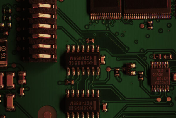
1. Schematics
It is a diagram of components, connections, and circuits that are laid out in an easy-to-understand way. It’s essential while designing a PCB layout as it helps engineers understand & construct the system of the circuit. Modern schematics must also incorporate component data that supports simulation models (IBIS, SPICE) for integrity analysis.
2. High-Frequency Signals
The PCBs that support higher frequencies have special requirements. Most of the interfaces used today operate at more than 50 MHz, making it essential to have some knowledge of frequencies to avoid issues with high signals. With the advancement in technology, the frequency of signals has become significantly higher, with many now operating in the Gigahertz (GHz) range (e.g., DDR5, PCIe Gen 5). Therefore, there is a need to understand signal propagation and treat traces as Transmission Lines.
This requires designing for Controlled Impedance by carefully defining the trace width and stack-up to maintain a specific characteristic impedance.
Also, it would help if you bridged the gap between analog & digital design. If you offer a professional PCB layout service, this high-speed expertise is non-negotiable.
3. Routing Signal & Placement of Components
When it comes to the placement of components & signal routing, one needs to follow the direction in which the signal & current flow in the PCB board design.
Make sure that you maintain a distance between the digital and analog signals. The analog circuits are sensitive to a digital signal and can even lead to disruptions on the analog side.
Beyond SI, placement must optimize the Power Delivery Network (PDN) by placing decoupling capacitors immediately adjacent to high-speed IC power pins to manage Power Integrity.
Steps Involved in PCB Designing
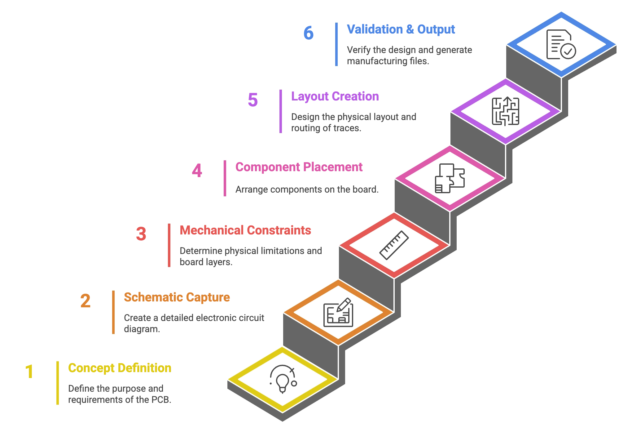
PCB designing plays a quintessential role at every point of the printed circuit board production process. Creating a PCB design board includes six basic steps that align with the core Design Engineering Phase of the overall manufacturing workflow.
To see how these six steps fit into the larger product lifecycle, refer to the industry workflow chart below:
1. Concept Definition and Requirements
Once you have identified the need for a PCB, the next step is to conceptualize the board. The initial phase involves defining the PCB’s functions and interconnection with other circuits, features, placements in the final product, and dimensions. Also, one needs to consider the approximate range of temperature and other environmental factors (e.g., vibration tolerance) in which it will operate. This phase establishes the block diagram and the overall system architecture.
2. Schematic Capture and Component Selection
Once you’re done with the concept, the next step is to draw the circuit schematic based on the finalized concept. It includes all the information needed for the board’s electrical components to function appropriately. Not only this, but it must also include the details, such as component name, rating, value, and manufacturer part number. When creating a schematic, don’t forget to create a bill of materials containing information on all the components you need for the PCB. The schematic must be ready for simulation, requiring accurate component data that supports simulation models (IBIS, SPICE).
3. Define Mechanical Constraints & Stack-up
You need to define Mechanical constraints such as Board dimension, thickness, cutouts, mounting holes, Keepout regions, Mating and I/O connector locations. Crucially, the PCB Stack-up (layer count and material) must be finalized here as it is the foundation for controlled impedance and dictates trace impedance and routing capacity.
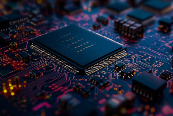
4. Component Footprint Creation & Placement
The next and very critical step in designing a PCB layout is the component’s placement. This stage involves creating accurate footprints for all components. A proper component placement ensures good electrical connection between Circuits and as well as enabling the PCB to be assembled and tested efficiently. The modern approach is Constraint-Driven, prioritizing thermal management, signal flow, and the proximity of decoupling capacitors for high-speed components.
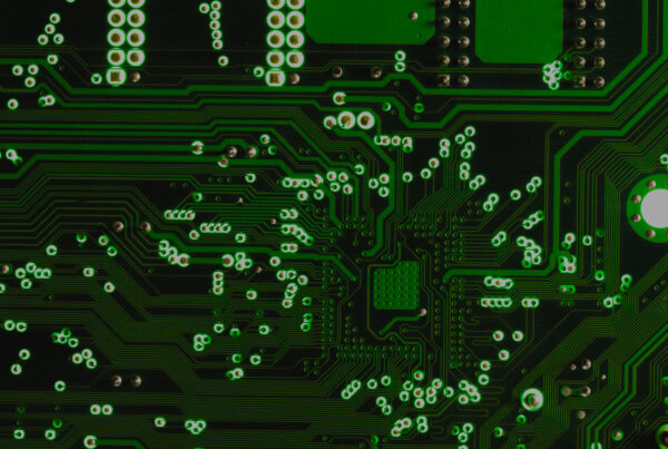
5. Layout Creation and Routing
The next important and tedious task in PCB design board layout is routing. This stage covers the creation of the final physical layout and copper pours. The routing determines the performance of high-speed interfaces, RF, analogue and high-power signals. A good routing between circuits improves the Signal and Power Integrity of the PCB. This is achieved through techniques like differential pair routing and managing skew control. While the electrical requirements are taken care of, all Design for Manufacturing (DFM) related constraints must be addressed to improve PCB fab yield.
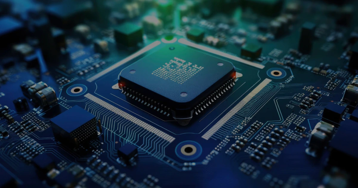
6. Validation and Output File Generation
This is the final step; after you’ve completed the design, you must run a series of Quality and Manufacturing (DRC) checks to meet all the requirements. This includes detailed Signal Integrity (SI) and Power Integrity (PI) Simulation on critical nets. The design gets completed once the checks are passed, but if not, you have to go back to the previous phases, where you need to make changes and adjustments. After passing DFM checks, the final outputs (Gerber files, drill files, BOM, etc.) are generated, preparing the design for the fabrication phase.
PCB Layout Techniques for Minimizing Crosstalk and Electromagnetic Interference (EMI)
How Tessolve Provides Turnkey Solutions for PCB Design Service?
As the leading semiconductor engineering solution provider, Tessolve is determined to serve clients and meet their needs. We develop ATE system and the evaluation boards that help our customers evaluate their product functionality before mass production. We provide the board developments with a team of experts in High-Speed Processors, Analog, RF domains, and Mixed signals. We ensure the perfect design through a combination of hardware engineering, advanced simulation, and PI Optimization, delivering a leading PCB layout service that gets you the best PCB design board that you want.
For better assistance from our experienced engineers, email us today sales@tessolve.com
FAQ
1. What is the difference between PCB layout and PCB design?
PCB design refers to the complete engineering process, including concept, schematics, component selection, stack-up planning, simulations, and final validation.
PCB layout is a part of PCB design that focuses specifically on component placement, routing, copper pours, drill details, and converting the schematic into a physical board format.
2. Why is controlled impedance important in high-speed PCB designs?
Controlled impedance ensures signal integrity by maintaining consistent trace characteristics, preventing reflections, distortions, and timing issues in high-frequency interfaces like DDR, PCIe, and SerDes.
3. What factors influence the placement of components during PCB layout?
Component placement depends on signal flow, thermal management, power delivery, high-speed routing needs, analog–digital isolation, manufacturability, and proximity of decoupling capacitors to IC power pins.
4. How does routing impact PCB performance?
Routing directly affects signal integrity, power integrity, EMI/EMC behavior, and overall device reliability. Techniques like differential pair routing, skew control, and avoiding impedance discontinuities are essential.