As data demands surge exponentially in AI workloads, cloud computing, and high-performance systems, traditional electronic interconnects are reaching their physical and thermal limits. Enter photon-driven ICs, a transformative solution powered by silicon photonics that brings light-speed data transmission directly onto the chip. With communication speeds now reaching 38 terabits per second (Tbps) and beyond, silicon photonics is not only redefining data transfer efficiency but also reshaping the future of chip design.
This blog delves into how photon-driven integrated circuits are revolutionizing on-chip communication and what this means for the next generation of computing architectures.
The Bottleneck of Electrical Interconnects
In classical computing architecture, metal interconnects carry electrical signals between different parts of a chip or between chips. However, as processing units scale and transistor counts rise, these interconnects become increasingly problematic due to:
- Resistance and capacitance effects lead to signal degradation.
- Thermal challenges, as higher bandwidth means more power and heat.
- Latency issues are limiting performance in parallelized and distributed computing environments.
Even with innovations like chiplet-based architectures and 2.5D/3D IC packaging, the physical limitations of copper wiring are hindering overall system throughput.
Enter Silicon Photonics: Light at the Heart of Chips
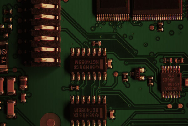
Silicon photonics leverages optical signals instead of electrical ones to move data. By integrating photonic components, such as waveguides, modulators, and detectors, into silicon chips, engineers can transmit data using light across on-chip and chip-to-chip interfaces.
Key advantages include:
- Higher bandwidth density: Optical links can carry more data per unit area.
- Lower power consumption: Less energy is lost as heat compared to metal interconnects.
- Reduced electromagnetic interference: Optical signals are immune to crosstalk and noise.
The transition to light-based communication directly on silicon is unlocking communication rates up to 38 Tbps and is forecasted to grow even further.
Inside Photon-Driven ICs: How They Work
A typical photon-driven IC integrates both electronic and photonic components on a common silicon substrate. Here’s how data flows:
- Electronic Signal Generation: Traditional transistors process digital signals.
- Electrical-to-Optical Conversion: A modulator converts the signal into an optical pulse.
- Light Transmission: Data moves through nano-scale waveguides at the speed of light.
- Optical-to-Electrical Conversion: A photodetector receives the light and converts it back to electrical form for processing.
Thanks to advances in CMOS-compatible photonic fabrication, these photonic components can now be manufactured using conventional silicon foundry processes, making it scalable and cost-effective.
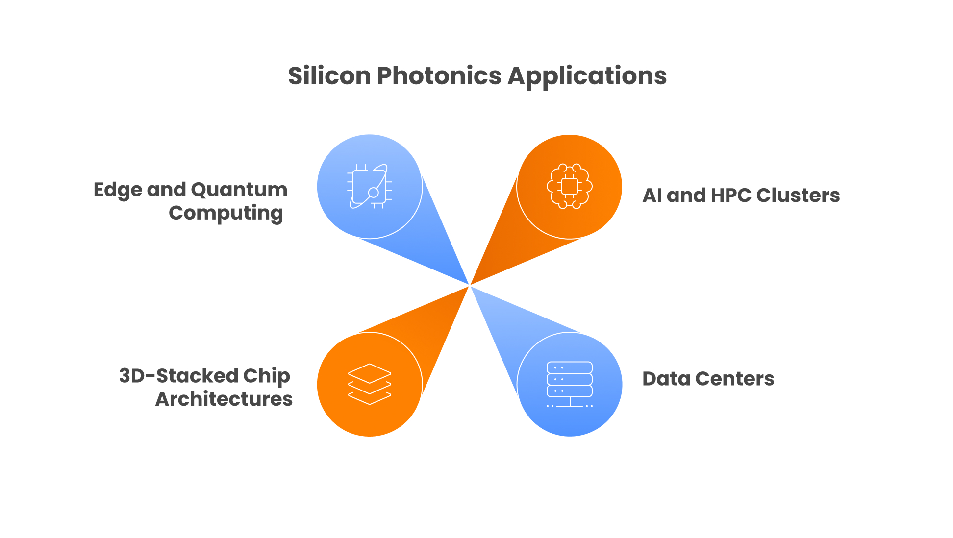
1. AI and HPC Clusters
Photon-driven ICs drastically cut interconnect latency in machine learning training clusters, enabling better parallelism across GPUs, CPUs, and AI accelerators.
2. Data Centers
Silicon photonics supports faster inter-rack and intra-chip communication, reducing the energy and hardware footprint of modern hyperscale data centers.
3. 3D-Stacked Chip Architectures
As chip design evolves toward vertical stacking, photonics-based interposers enable high-throughput, thermally efficient communication between chiplets.
4. Edge and Quantum Computing
Photonics opens the door for secure, low-latency communication in specialized computing systems, including quantum and neuromorphic chips.
Technical Challenges and Innovations
Despite its promise, silicon photonics still faces several hurdles:
- Integration complexity: Combining photonics and electronics requires advanced co-design strategies.
- Thermal tuning: Maintaining wavelength stability across temperatures is difficult.
- Packaging limitations: Coupling light efficiently into and out of the chip needs precision alignment.
- Yield and variability: Fabricating nano-scale optical components with consistent performance is still a maturing process.
To address these, research is ongoing in new materials (like germanium and III-V semiconductors), advanced lithography techniques, and AI-assisted photonic layout tools.
Silicon Photonics and the Future of Chip Design
Photon-driven ICs are shaping the future of VLSI chip design by introducing a fundamentally new dimension, light. This requires engineers to rethink the traditional floorplanning, routing, and energy budgeting in chips.
Key trends include:
- Co-design frameworks that simulate and optimize electrical and photonic circuits in unison.
- Photonic EDA tools that integrate with traditional VLSI workflows.
- AI-enhanced placement algorithms to manage both photonic waveguides and electronic interconnects.
Leading chip design companies are investing in hybrid electro-photonic SoCs that merge logic processing with ultra-fast optical communication, particularly for AI inference and training chips.
Advancements in RISC-V Architecture for Custom Chip Design
Why Tessolve is Your Partner for Advanced Chip Design Innovation
At Tessolve, we understand that pushing the boundaries of data throughput requires more than incremental improvements; it demands transformative innovation. Our comprehensive VLSI chip design services are tailored to meet the demands of next-gen architectures, including photon-driven and silicon photonics-based systems.
Our capabilities include:
- End-to-end ASIC and SoC design services
- Advanced package and interposer design for optical and 3D integration
- Custom silicon validation and testing frameworks
- Co-simulation and modeling tools for mixed-signal and photonic ICs
- Expertise across multi-die and chiplet architectures
We bring together deep expertise in chip design and system-level integration to enable high-speed, low-latency, and energy-efficient solutions that scale. Whether you’re exploring silicon photonics or building a cutting-edge AI accelerator, Tessolve is equipped to support your innovation from design to deployment.
Conclusion: Light-Speed Chips Are No Longer Science Fiction
Photon-driven ICs mark a revolutionary leap forward, enabling chips that can communicate at 38 Tbps and beyond while reducing energy consumption and heat. As the silicon photonics ecosystem matures, it is poised to become a mainstay in future computing platforms, from cloud servers to quantum processors.
Integrating photonics into chip architecture also signals a shift in how engineers think about interconnects, packaging, and architecture. The future of chip design will be defined not just by logic density or node size, but by how efficiently data can move, at the speed of light.
With trusted partners like Tessolve and the growing support from top chip design companies, the next era of VLSI chip design will be more connected, efficient, and faster than ever.