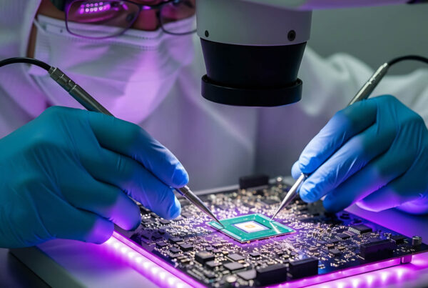

The demand for highly efficient and reliable VLSI chips has grown exponentially in the fast-paced world of chip design services. VLSI chip design, encompassing various stages from conception to manufacturing, plays a crucial role in achieving optimal performance and functionality. With memory now occupying up to 90% of a modern System-on-Chip (SoC) area, memory testing holds a significant position among the critical components of VLSI chip design. This article will delve into the importance of memory testing in digital VLSI designs and how it contributes to the overall success of VLSI chip development and deployment.
Understanding VLSI Chip Design
VLSI – Very Large-Scale Integration, refers to the process of designing complex integrated circuits by incorporating a large number of transistors onto a single chip. VLSI chip design involves multiple stages, including architecture design, logic design, VLSI layout design, and fabrication. The primary objective of VLSI chip design is to achieve high performance, low power consumption, and reduced area utilization. As we move into 2nm and 3nm process nodes, the focus has shifted toward Gate-All-Around (GAA) architectures, which require even more precise memory-logic integration.
Memory Testing: A Critical Aspect of VLSI Chip Design
Memory elements, such as Random Access Memory (RAM) and Read-Only Memory (ROM), are integral parts of VLSI chips, serving as storage units for data and instructions. These memory elements must be thoroughly tested to ensure they function reliably under various operating conditions. Memory testing in digital VLSI designs involves a set of techniques and methodologies to verify the integrity, performance, and functionality of the memory blocks present in the chip.
At modern nodes, traditional static fault models are no longer sufficient; designers must now address “dynamic faults,” defects that only manifest during high-speed operations. Tesslove has a robust test setup that provides you with 24×7 testing assistance. We provide you with IP and SOC-level Verification using C/C++ and SV-UVM methodologies. We are integrated with tools like formal verification and PSS for verification productivity.
The Importance of Memory Testing
- Fault Detection: Memory testing helps identify potential faults or defects in memory elements, ensuring the chip operates flawlessly. Beyond standard “Stuck-At” faults, modern testing identifies complex “Coupling” and “Neighborhood Pattern Sensitive Faults” (NPSF). Faulty memory cells can lead to data corruption, system crashes, or even catastrophic failures. VLSI chip.
- Performance Optimization: Memory testing enables designers to evaluate the performance characteristics of memory elements, such as access time, read and write speeds, and power consumption. Thermal-aware testing is now vital, as dense memory stacks in 3D ICs can generate localized “hotspots” that degrade performance.
- Yield Enhancement: VLSI layout design fabrication involves complex manufacturing processes that can introduce defects in the memory elements. Conducting extensive memory testing during the design phase can identify potential fabrication-related issues early on, allowing for modifications and improvements that result in higher chip yield.
- Compatibility Assurance: Memory testing ensures compatibility between the VLSI chip and its intended application environment. This is critical for automotive-grade chips, where memory must adhere to strict functional safety (ISO 26262) standards.
Advanced Memory Testing Techniques
To accomplish comprehensive coverage, designers employ specialized techniques:
- Built-In Self-Test (MBIST): Modern MBIST architectures are now “AI-driven,” using machine learning to adaptively generate test patterns that target high-risk areas of the memory array. BIST allows for on-chip testing without external equipment.
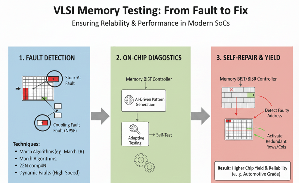
As shown in the diagram above, a modern MBIST architecture integrates a test controller directly on-silicon to generate patterns and compare results, ensuring high reliability without slowing down production.
- March Algorithms: These are widely used for detecting common memory faults. Advanced “March LR” and “March SS” algorithms are now used to achieve 22N complexity, providing superior coverage for linked and dynamic faults.
- Memory Built-In Self-Repair (MBISR): Also known as Built-In Redundancy Analysis (BIRA), these techniques provide automatic repair mechanisms, allowing faulty memory elements to be bypassed using spare rows or columns during runtime.
Why Choose Us?
Tessolve is a leading provider of chip design services. Memory testing is given the utmost importance in the digital VLSI design process. With a deep understanding of the complexities involved in memory testing, Tessolve offers comprehensive solutions that ensure the reliability and performance of VLSI chips. By leveraging advanced memory testing techniques and a team of skilled engineers, we strive to deliver advanced VLSI chip designs that exceed industry standards.
We specialize in complex IPs and subsystems in Graphics, PCIE-Gen5, Processors, CXL3.0, LPDDR4, GDDR6, and Automotive domains. Our team leverages AI-driven automated debugging and power-aware verification to shorten time-to-market. If you’re seeking chip design services that prioritize memory testing and offer end-to-end solutions for VLSI chip design, Tessolve is your ideal partner.
Increased Importance of VLSI Design Ecosystem in India for Worldwide Semiconductor Industry
Conclusion
Memory testing plays a pivotal role in the development of VLSI chips. By ensuring the integrity, performance, and compatibility of memory elements, designers can enhance the overall reliability and functionality of digital VLSI designs. By adopting advanced memory testing techniques, chip design services can achieve higher chip yields, optimize performance, and deliver high-quality VLSI chips that meet the ever-increasing demands of the industry.
Contact Tessolve today to explore how their expertise in memory testing and VLSI chip design can help you achieve your goals in the ever-evolving landscape of semiconductor technology.
Frequently Asked Questions
1. What is the most common fault detected during memory testing?
While “Stuck-At” faults are common, “Coupling Faults,” where one cell’s state affects another, are the primary focus in high-density designs.
2. How does AI help in memory verification?
AI-driven tools predict potential failure points and generate targeted test patterns, reducing the time spent on manual debugging.
3. Which type of memory is usually faster in VLSI design?
SRAM is significantly faster than DRAM because its flip-flop structure provides instant access without requiring periodic refresh cycles.
4. What are the fundamental manufacturing test principles in VLSI?
Testing relies on three core principles: establishing observability, maintaining controllability, and maximizing fault coverage using standardized models like stuck-at.