In the complex field of PCB hardware design, grasping transmission line theory is essential for maintaining signal integrity in high-speed circuits. Transmission lines facilitate smooth signal propagation by controlling impedance, minimizing loss, and reducing distortion. As electronic systems become faster and more intricate, the demand for precise transmission line design increases significantly. Engineers must not only understand the fundamental principles but also know how to implement advanced configurations to meet industry requirements.
Modern PCB systems now operate at extremely high data rates, where signal integrity challenges increase due to tighter layouts and high-frequency interfaces. Microstrip and stripline configurations are two fundamental transmission line types employed to achieve controlled impedance and predictable performance. Let’s delve into these concepts and unravel their significance in modern PCB design.
Basics of Transmission Line Theory
Transmission lines serve as pathways for signals, enabling them to travel from one point to another. These lines ensure minimal loss and distortion by controlling impedance, which is influenced by the line’s geometry, materials, and frequency of operation. For PCB hardware professionals, ensuring impedance matching is essential to avoid reflection, signal degradation, and electromagnetic interference (EMI).
The critical parameters in transmission line theory include:
- Impedance (Z0): The characteristic impedance must match source and load to avoid reflections.
- Propagation Delay: Signal travel time depends on the dielectric material and line geometry.
- Signal Integrity: Influenced by cross-talk, attenuation, and EMI.
At higher frequencies, even small discontinuities in the transmission path can significantly impact signal quality, making precise design practices essential.
Microstrip vs. Stripline: Key Differences
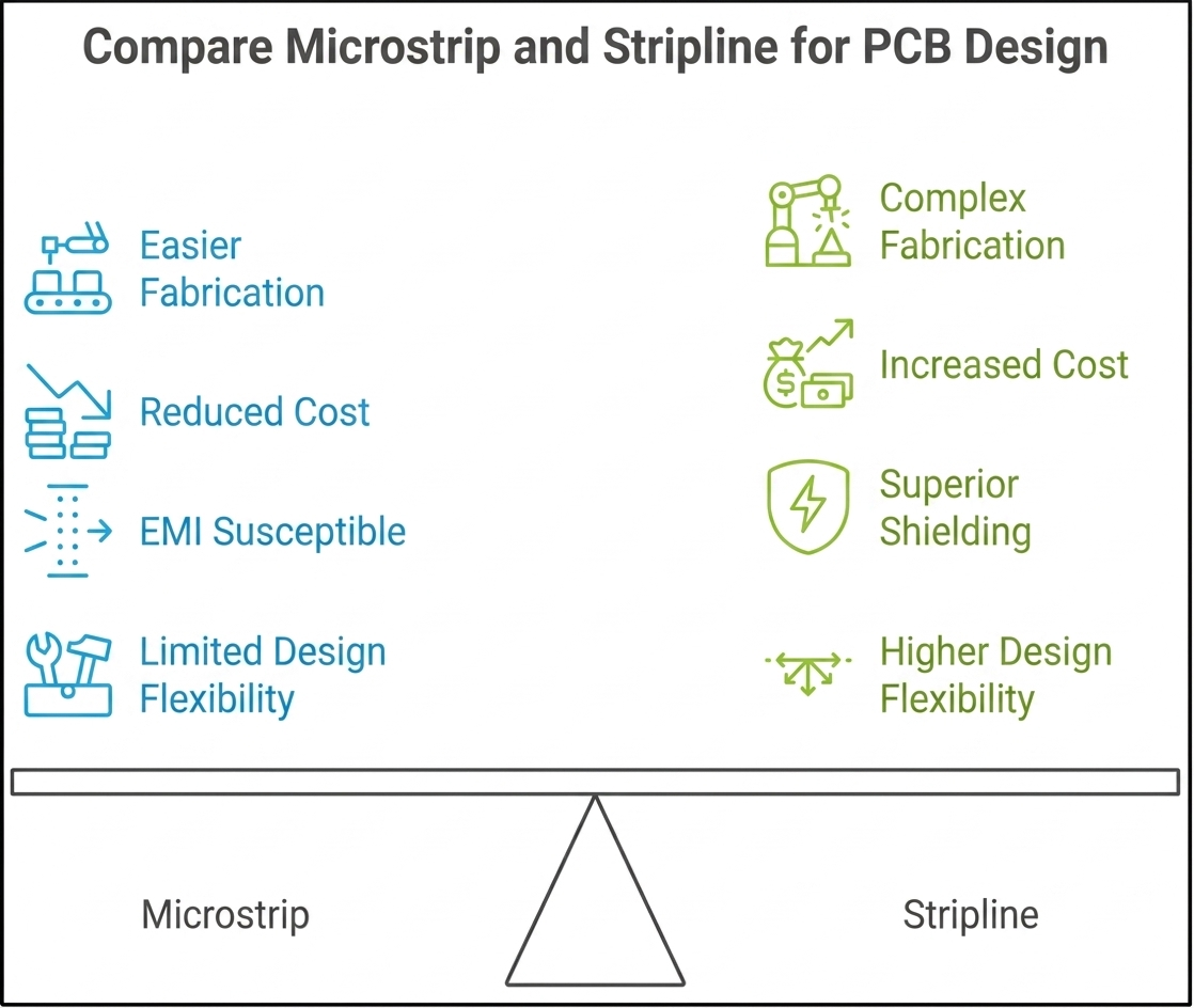
Microstrip
A microstrip transmission line comprises a conductor placed above a ground plane, separated by a dielectric layer. Found on the outer layers of a PCB, microstrip lines are straightforward to fabricate and inspect.
Advantages:
- Easier to manufacture and modify.
- Reduced cost compared to stripline.
- Direct exposure allows for convenient RF tuning.
Challenges:
- Susceptible to external EMI.
- Requires careful design to mitigate signal losses due to fringing fields.
Applications:
Microstrip is commonly used in RF circuits, antennas, and simpler PCB hardware design configurations.
Stripline
Stripline places a conductor between two ground planes, fully enclosed by the dielectric material. This structure is typically used in inner PCB layers.
Advantages:
- Superior shielding from external noise.
- Higher design flexibility for complex multilayer PCBs.
- Consistent impedance characteristics.
Challenges:
- Increased manufacturing complexity and cost.
- More difficult inspection and troubleshooting due to internal placement.
Applications:
Stripline is ideal for high-speed digital circuits and sensitive signal applications requiring robust noise immunity. It is commonly preferred in dense multilayer PCBs where signal isolation and EMI control are critical.
Impedance Control in PCB Design
Controlled impedance ensures signal integrity across transmission lines. For both microstrip and stripline, factors like line width, spacing, and the dielectric constant of materials play a crucial role. Tools like electromagnetic simulation software aid in designing transmission lines that meet the desired specifications. By partnering with a reliable hardware design company, engineers can optimize impedance and reduce development cycles.
Key Considerations
- Dielectric Material: Impacts signal speed and loss.
- Line Geometry: Determines impedance.
- Ground Planes: Ensure signal return paths are effective to minimize crosstalk.
Impedance mismatches often lead to reflections and signal degradation. For efficient transmission, the characteristic impedance must align with the source and load, especially in high-frequency systems. Modern PCB design increasingly relies on accurate modeling and stack-up planning to maintain impedance consistency across complex multilayer boards.
Signal Integrity and EMI Considerations
Signal integrity issues stem from reflections, losses, and noise coupling. Effective transmission line design mitigates these problems:
- Minimize Crosstalk: Proper spacing between traces and ground return paths.
- Reduce EMI: Shielding layers and careful component placement help limit interference.
- Material Selection: Low-loss dielectric materials reduce attenuation.
The careful implementation of transmission lines ensures signal reliability, especially in electrically noisy environments. With increasing signal speeds, even minor layout imperfections can introduce noise, making EMI control and signal integrity planning essential from the early design stage.
Role of Design Tools and Simulation
In modern PCB hardware workflows, design tools facilitate accurate modeling of microstrip and stripline configurations. Advanced software supports:
- Simulating signal propagation.
- Verifying impedance control.
- Predicting EMI and signal loss effects.
Software tools such as HFSS and ADS allow for detailed simulations, empowering engineers to refine designs before physical prototyping. These tools are indispensable for minimizing iterations and achieving first-pass success in PCB design.
Real-World Applications and Trends
Microstrip and stripline designs continue to play a critical role across a wide range of industries:
- Telecommunications: High-speed data transmission, RF front-end modules, and antenna feed networks
- Automotive: ADAS systems, radar modules, and in-vehicle high-speed communication networks
- Aerospace: Reliable signal transmission in electrically noisy and high-reliability environments
Emerging Trends
High-Speed Interfaces
Modern PCBs support ultra-high-speed links and multi-gigabit data rates, making precise impedance control critical for signal integrity.
Chiplet and System-Level Design
Chiplet-based architectures and dense interconnects require tighter control over transmission lines and PCB stack-ups.
Advanced Materials and Stack-Ups
Use of low-loss dielectrics and optimized multilayer designs helps reduce signal loss and improve performance.
Miniaturization and Density
Smaller devices lead to denser routing and a higher risk of EMI and crosstalk, requiring more accurate layout strategies.
Tessolve: A Leader in Hardware Design Solutions
When it comes to the seamless execution of PCB hardware design, Tessolve stands out as a trusted partner. Specializing in comprehensive PCB design services, we offer cutting-edge solutions tailored to meet the demands of high-performance circuits. From schematic capture to layout design and simulation, our team ensures optimal performance and reliability.
Tessolve’s expertise spans:
- Designing high-speed interfaces.
- Delivering robust solutions for multilayer PCB stacks.
- Ensuring first-pass success with stringent quality checks.
By leveraging advanced simulation tools and modern design methodologies, Tessolve helps address complex signal integrity and EMI challenges efficiently.
Our global presence, state-of-the-art facilities, and robust engineering expertise empower businesses to overcome design complexities and achieve unparalleled quality. Whether your need is a simple two-layer board or an intricate 60-layer design, Tessolve delivers. Contact us now and explore the difference with Tessolve, your partner in engineering excellence.
Channel Modeling and Simulation for High-Speed PCB Design Verification
Let’s Conclude
Understanding microstrip and stripline transmission lines is essential for achieving signal integrity in PCB hardware design. By applying the right design techniques and using advanced tools, engineers can reduce noise, improve performance, and ensure reliability.
As electronic systems continue to evolve, mastering transmission line theory will remain crucial. It enables engineers to design high-speed, high-performance PCBs that meet modern industry requirements.
Frequently Asked Questions
1. What is the difference between stripline and microstrip transmission lines?
Microstrip is placed on the outer PCB layer and exposed to air, making it easier to access but more prone to EMI, while stripline is embedded between ground planes, offering better shielding and stable impedance.
2. What are the theoretical effects of impedance mismatch on signal integrity in transmission lines?
Impedance mismatch causes signal reflections, standing waves, and energy loss. This leads to waveform distortion, timing errors, reduced signal quality, and potential failure in high-speed digital or RF systems.
3. What are the structural details and applications of stripline?
A stripline consists of a conductor sandwiched between two ground planes within a dielectric. It is used in high-speed digital circuits, RF systems, and applications requiring strong noise immunity.
4. How can engineers reduce EMI in transmission lines?
Engineers reduce EMI using proper grounding, shielding, controlled impedance routing, trace spacing, and optimized PCB stack-up design.
5. When should stripline be preferred over microstrip?
Stripline is preferred in high-speed and noise-sensitive designs where strong shielding, stable impedance, and minimal EMI are required.