
In today’s technology-driven world, VLSI design has become a cornerstone of modern electronics, enabling the creation of highly integrated circuits for a variety of applications. Achieving optimal PPA (Power, Performance, and Area) is a critical goal for every VLSI design engineering team. PPA serves as the key metric for evaluating the quality and efficiency of a VLSI circuit and dictates its competitiveness in the market. In this blog, we will explore proven strategies and methodologies to improve PPA in VLSI physical design and other stages of the design process.
Understanding PPA in VLSI Design
Before diving into optimization techniques, it’s essential to understand what PPA stands for:
- Power: This represents the total energy consumed by the VLSI circuit, including static and dynamic power components. Power optimization is crucial for enhancing battery life in portable devices and reducing energy costs for large-scale computing systems.
- Performance: Measured in terms of operating frequency and speed, performance determines how fast the VLSI circuit executes its tasks. High-performance circuits are essential for applications like high-speed computing and data processing.
- Area: Area refers to the silicon real estate occupied by the circuit on the chip. Minimizing area reduces costs and enables higher integration levels, which is a fundamental goal in VLSI design engineering.
Achieving a balance among these three metrics is a complex but rewarding challenge that requires expertise in VLSI physical design and a deep understanding of system-level requirements.
Key Strategies to Improve PPA
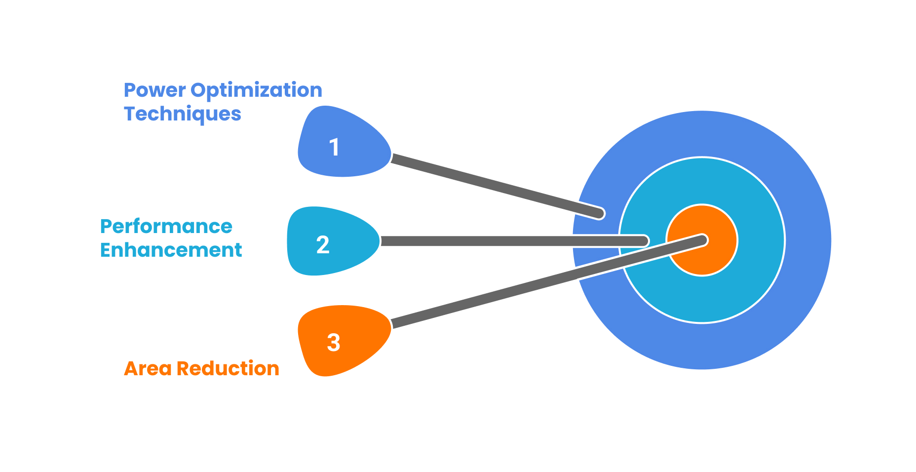
1. Power Optimization Techniques
Power optimization can be achieved at multiple levels in the VLSI design process:
- Clock Gating: Designers can significantly reduce dynamic power consumption by disabling the clock signal to inactive circuit parts. This technique is widely used in VLSI physical design to manage power budgets effectively.
- Voltage Scaling: Lowering supply voltage is a proven method for reducing power, as power consumption is proportional to the square of the voltage. Dynamic Voltage and Frequency Scaling (DVFS) is a popular implementation.
- Multi-Vt Design: Utilizing cells with multiple threshold voltages allows a trade-off between power and performance. High-Vt cells reduce leakage power, while low-Vt cells enhance performance.
- Power Gating: Power gating involves turning off power to inactive circuit blocks, thereby reducing leakage current. This is particularly effective for battery-powered devices.
2. Performance Enhancement
Performance optimization ensures the VLSI circuit meets the required operating speeds. Techniques include:
- Critical Path Optimization: Identifying and minimizing delays along the critical paths of the circuit can significantly boost performance. This involves efficient placement and routing during VLSI physical design.
- Pipeline Stages: Increasing pipeline stages can improve throughput, although it may introduce latency. Balancing these factors is crucial.
- Clock Tree Synthesis (CTS): A well-optimized clock tree minimizes skew and jitter, ensuring reliable performance.
- Process Technology Scaling: Transitioning to advanced process nodes like 5nm or 3nm can unlock higher performance potential due to reduced parasitics and improved transistor characteristics.
3. Area Reduction
Minimizing the area of a VLSI circuit is essential for reducing costs and increasing functionality per chip. Area optimization strategies include:
- Standard Cell Libraries: Using dense standard cell libraries with compact layouts helps save area without compromising performance.
- Placement and Routing Optimization: Efficient floorplanning and routing during VLSI physical design can reduce interconnect lengths and save valuable silicon area.
- Design for Manufacturability (DFM): Ensuring the design adheres to DFM guidelines minimizes the risk of yield loss, indirectly reducing the cost per chip.
- Logic Optimization: Techniques like Boolean simplification, resource sharing, and logic restructuring can reduce the circuit’s gate count and area requirements.
Role of Tools and Methodologies
Advanced tools and methodologies are indispensable for achieving superior PPA in VLSI design. Popular EDA (Electronic Design Automation) tools like Synopsys, Cadence, and Mentor Graphics provide powerful features for:
- Design Space Exploration: Tools like Design Compiler and Innovus allow engineers to explore multiple design trade-offs early in the development cycle.
- Static Timing Analysis (STA): Ensuring the circuit meets timing constraints is critical for performance. Tools like PrimeTime are widely used.
- Power Analysis: Tools like PowerPro and Voltus enable accurate power estimation and optimization.
- Sign-Off Checks: Final verification steps, including Design Rule Checks (DRC) and Layout Versus Schematic (LVS), ensure the design is manufacturable and meets specifications.
By leveraging these tools effectively, VLSI design engineering teams can achieve remarkable improvements in PPA.
Importance of Collaboration in VLSI Design Engineering
Collaboration is key to achieving PPA goals. Teams involved in architecture, logic design, and VLSI physical design must work closely to ensure the design meets system-level requirements. Cross-functional collaboration allows for the following:
- Early Identification of Bottlenecks: Issues related to power, performance, or area can be identified and addressed in the early stages of VLSI design.
- Efficient Iterations: By integrating feedback loops across teams, design iterations become more targeted and efficient.
- Better Trade-Off Decisions: Collaborative decision-making ensures that trade-offs among power, performance, and area are optimized for the end application.
From Concept to GDSII: A Deep Dive into the VLSI Design Flow
The journey of VLSI design begins with an idea and culminates in the physical implementation of the chip, referred to as GDSII. The design flow involves multiple stages, each critical to achieving optimal PPA:
- Specification and Architecture: The design starts with defining the specifications and creating a high-level architecture. This involves determining system requirements like performance, power, and area.
- RTL Design: Register Transfer Level (RTL) design involves coding the functionality of the chip using hardware description languages like Verilog or VHDL. Functional verification is performed at this stage.
- Synthesis: RTL is translated into a gate-level netlist using synthesis tools. The netlist is optimized for timing, area, and power.
- Physical Design: This involves placement, routing, clock tree synthesis, and optimization of the netlist to meet physical and electrical constraints.
- Sign-Off: Final verification steps include timing analysis, power analysis, and layout checks to ensure the design meets all specifications before being sent for fabrication.
Understanding the intricacies of each phase is vital for VLSI design engineering teams to deliver high-quality chips.
10 Ways Low Power VLSI Design Enables a Smarter and Greener Tomorrow
Learn more about the VLSI Design Flow
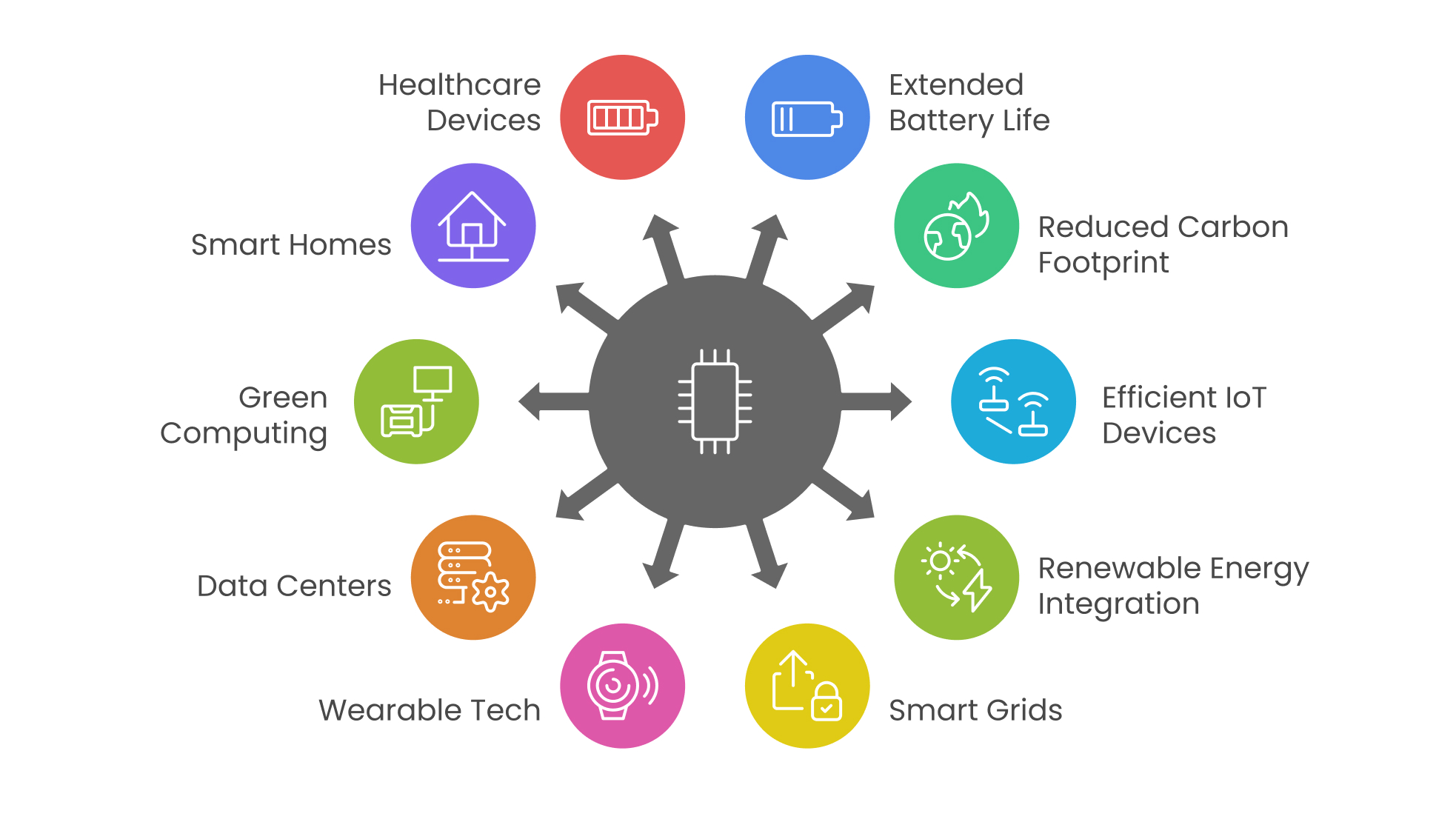
Low-power VLSI design is revolutionizing the electronics industry by enabling energy-efficient solutions for a sustainable future. Here are ten ways it contributes to a smarter and greener tomorrow:
- Extended Battery Life: Optimized power consumption allows portable devices to operate longer without frequent recharging. This is crucial for consumer electronics and IoT devices.
- Reduced Carbon Footprint: Lower energy usage results in reduced emissions, contributing to environmental sustainability and aligning with global green initiatives.
- Efficient IoT Devices: Low-power designs are critical for IoT devices, enabling extended operation with minimal energy and ensuring reliability in remote deployments.
- Renewable Energy Integration: Energy-efficient designs support renewable energy systems, improving their viability and effectiveness in smart grid applications.
- Smart Grids: Low-power VLSI enables the development of intelligent grids that optimize energy distribution, reducing waste and enhancing energy availability.
- Wearable Tech: Power-efficient chips enhance the usability of wearables by reducing the need for frequent charging, promoting user convenience.
- Data Centers: Reducing server power consumption minimizes operational costs, lowers cooling requirements, and boosts energy efficiency in cloud computing.
- Green Computing: Power-efficient processors enable the development of environmentally friendly computing systems, which is crucial for sustainable IT infrastructures.
- Smart Homes: Energy-efficient VLSI designs power devices that automate and reduce energy use in households, improving overall energy efficiency.
- Healthcare Devices: Low-power VLSI extends the life of medical devices, improving patient outcomes by ensuring long-lasting and reliable operation in critical healthcare environments.
Know about 10 Ways Low Power VLSI Design Enables Smarter and Greener Tomorrow
Innovative Approaches in VLSI Chips Memory Management: Design Strategies
Memory management plays a pivotal role in the efficiency and performance of VLSI circuits. Innovative approaches in this domain include:
- Hierarchical Memory Design: Using multi-level memory hierarchies reduces latency and power consumption by enabling faster access to frequently used data.
- Error Correction Techniques: Incorporating error correction codes (ECC) ensures data integrity, reducing the need for redundant memory accesses and improving reliability.
- Dynamic Voltage and Frequency Scaling (DVFS): Adjusting voltage and frequency based on workload minimizes power usage in memory systems, making them more energy-efficient.
- 3D Memory Integration: Stacking memory in 3D architectures reduces area while increasing bandwidth, enhancing performance in compact designs.
- Low-Power DRAM and SRAM: Optimized memory cell designs reduce leakage power, significantly improving energy efficiency in modern VLSI systems.
- Cache Optimization: Designing smarter caching mechanisms improves performance and reduces energy consumption, particularly in high-performance computing systems.
- Data Compression: Storing compressed data minimizes memory usage, enhancing area efficiency while maintaining performance.
- Power Gating: Turning off unused memory blocks reduces static power, contributing to overall system energy savings.
These strategies enhance the overall efficiency of VLSI design engineering, enabling smarter and more sustainable electronic systems.
Read about Innovative Approaches in VLSI Chips Memory Management
Bridging the Gap Between Innovation and Sustainability
As technology evolves, achieving better PPA in VLSI design becomes a dynamic process requiring continuous innovation and adaptation. Companies that prioritize energy-efficient and high-performance solutions are better positioned to succeed in today’s competitive market. Furthermore, aligning VLSI design engineering strategies with sustainability goals ensures long-term benefits for both businesses and the environment.
This convergence of innovation and sustainability highlights the need for comprehensive approaches that address power, performance, and area simultaneously. By leveraging advanced tools, methodologies, and collaborative design frameworks, VLSI design teams can create solutions that meet modern demands while paving the way for future advancements.
Know about Sustainability in Semiconductor Engineering: Advancement and Innovations
Let’s Sum Up!
Achieving better PPA in VLSI design is a multifaceted challenge that requires a combination of technical expertise, advanced tools, and strategic collaboration. By focusing on power optimization, performance enhancement, and area reduction, VLSI design engineering teams can create efficient and cost-effective VLSI circuits that drive innovation across industries.
Partnering with Tessolve further amplifies your chances of success, providing the support and insights needed to excel in this ever-evolving field. With a clear focus on sustainability and efficiency, the journey to optimal PPA is a challenge that rewards innovation and collaboration in equal measure.