For decades, the system-on-chip (SoC) was king. Pack as many functions as possible onto a single monolithic die, push the node, and ride Dennard scaling. But physics, economics, and time-to-market pressures have changed the rules. Enter chiplet architectures, composable systems built from multiple smaller dies within one package. This paradigm is reshaping roadmaps for every top semiconductor company, every semiconductor design company, and the broader discipline of semiconductor engineering.
Why Chiplets, Why Now?
Three forces converged. First, reticle limits mean you can’t print chips beyond a certain area in one exposure, historically ~26 mm × 33 mm (≈858 mm²). That cap conflicts with increasing logic counts, wide memory interfaces, and larger accelerators.. Second, the cost curve at advanced nodes is steep; moving all IP to the newest node can be overkill. Third, time-to-market favors reuse and parallel development across teams and suppliers. Chiplets answer all three: break functions into smaller dies, place each on the optimal process, and integrate them in-package.
For a top semiconductor company, this means higher yield (smaller dies fail less often), mix-and-match process nodes (e.g., leading-edge logic beside mature analog), and faster iteration cycles. For a semiconductor design company, modularity enables differentiated products derived from common chiplet libraries. And for semiconductor engineering, the focus expands from single-die closure to multi-die integration, packaging, and system architecture.
The Role of Chiplets in Semiconductor Design: A Modular Approach
The Interconnect That Makes It Click
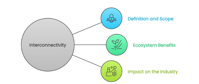
A modular system, such as chiplets, relies on seamless communication between dies. This is where Universal Chiplet Interconnect Express (UCIe) becomes a game-changer. Key aspects of UCIe:
1. Definition and scope
- Standardizes the die-to-die physical layer, protocols, software model, and compliance.
- Enables high-bandwidth, low-latency communication across organic substrates, 2.5D interposers, and 3D stacks.
2. Ecosystem benefits
- Creates an open marketplace for “plug-and-play” chiplets.
- Supports interoperability among vendors, driving faster innovation and broader adoption.
3. Impact on the industry
- For a semiconductor design company: shifts sourcing from in-house macro blocks to external, pre-verified chiplets with hardened PHYs and known-good-die (KGD).
- For semiconductor engineering: redefines verification boundaries, requiring system-level validation rather than only single-die testing.
- For a top semiconductor company: it reduces integration risks, shortens time-to-market, and enhances scalability.
Packaging is the New Performance
Chiplets depend on advanced packaging to deliver performance, scalability, and efficiency.
Key packaging approaches:
- 2.5D Interposers – high wiring density, ideal for HBM proximity.
- 3D Stacking – shorter interconnects, higher bandwidth, better efficiency.
- Fan-Out Packaging – extends beyond single-reticle limits, enabling large GPUs, AI accelerators, and memory-rich devices.
Engineering priorities:
- Thermal – manage heat across stacked or lateral chiplets.
- Power Integrity – handle multiple voltage domains and long redistribution traces.
- Signal Integrity – mitigate crosstalk, skew, and ensure high-speed die-to-die performance.
Why it matters:
For any top semiconductor company, co-optimizing packaging, interconnect, and power delivery is now as critical as process node selection. These are central semiconductor engineering tasks, not secondary concerns.
Architectural Freedom
Chiplets unlock new partitioning strategies:
- Heterogeneous integration: Pair bleeding-edge CPU tile(s) on N3/N2 with analog, RF, or I/O chiplets on cost-effective nodes, value without monolithic migration.
- Scalable products: Reuse a compute die across SKUs, varying only I/O or memory tiles to address market tiers.
- Domain specialization: Dedicated acceleration tiles for AI, security, or video offload that can evolve at their own cadence.
Constraints exist. Latency and energy per bit across die-to-die links aren’t free; software and firmware must account for topology. Cache coherency across chiplets, especially with heterogeneous memory hierarchies and disaggregated accelerators, requires careful protocol selection and QoS. And supply-chain complexity rises: more parts, more test flows, and more vendors.
Verification, Test, and KGD
Verification moves from single-die closure to system-level proof across chiplet boundaries. Pre-silicon emulation must model die-to-die behavior; post-silicon validation needs new bring-up sequences and observability points across tiles. Design-for-Test (DFT) extends to inter-die links, loopbacks, boundary scan, and built-in self-test (BIST) for KGD assurance, because one bad chiplet can sink a whole module.
A semiconductor design company that masters robust KGD flows, interconnect characterization, and multi-die ATPG gains a time-to-yield advantage. It’s exactly where the differentiation frontier sits today for a top semiconductor company executing volume programs.
Economics and Roadmaps
Chiplets rewrite the BoM and roadmap math. Yes, packaging and assembly costs rise, and yield interactions can complicate forecasting. But smaller dies at optimal nodes usually offset losses from monolithic reticle-edge designs, while SKU reuse amortizes NRE across a portfolio. The result is faster feature evolution, SKU agility, and lifecycle extensions by swapping in refreshed chiplets instead of respinning a massive SoC.
For teams practicing semiconductor engineering, that means earlier co-design between architecture, packaging, test, and operations, and tighter partnerships with OSATs, EDA vendors, and interconnect IP suppliers.
What to Do Next
- Adopt standards early. Target UCIe-compliant PHYs/links to de-risk multi-vendor integration.
- Invest in package-aware design. Elevate PI/SI/thermals to first-class citizens during partitioning.
- Industrialize KGD. Strengthen DFT/DFD for die-to-die observability and rapid bring-up.
- Build reusable chiplet libraries. Treat tiles as products with roadmaps, not just one-off program artifacts.
Do this, and your organization, whether a semiconductor design company or an aspiring top semiconductor company, can move from monolithic complexity to modular velocity.
3D ICs, Chiplets & HBM: How Packaging Is Driving the Semiconductor Roadmap
Why Tessolve for Chiplet-Era Programs
At Tessolve, we deliver end-to-end silicon solutions that map naturally to chiplet workflows, from RTL-to-GDSII chip design and DFT, to ATE test development and product engineering, to post-silicon validation and reliability qualification, and embedded/system design that brings multi-die systems to life. Our VLSI teams cover analog, digital, mixed-signal, and RF; our test engineering accelerates transition from prototype to high-volume; our labs de-risk reliability; and our embedded experts stitch hardware, firmware, and connectivity into complete products. Backed by rigorous quality systems and active ecosystem partnerships, we help you partition confidently, validate quickly, and scale reliably across advanced packages and UCIe-class interconnects.