In the ever-evolving world of semiconductor innovation, traditional system-on-chip (SoC) models are reaching their limits. As the demand for higher performance and smaller chip sizes continues to rise, 3D IC design using multi-die architectures is quickly becoming the preferred solution. From high-performance computing and artificial intelligence to mobile devices and wearables, the industry is undergoing a transformation, moving from monolithic designs to interconnected chiplets and heterogeneous integration.
This guide offers a practical look at how we’re transitioning from conventional SoCs to multi-die systems and what engineers, chip design companies, and systems architects must know to stay ahead.
Why the Shift from SoCs to Multi-Die Architectures?
System-on-chip designs have dominated for years, integrating numerous subsystems onto a single silicon die. However, as feature sizes shrink and transistor densities increase, issues like thermal dissipation, yield reduction, and cost per wafer have begun to challenge the viability of continued SoC scaling.
Multi-die architecture solves many of these issues by:
- Enabling heterogeneous integration: Different dies can use different process nodes (e.g., combining 7nm logic with 28nm analog).
- Improving yield and cost efficiency: Smaller dies yield better and can be manufactured independently, then assembled.
- Enhancing modularity and scalability: Reusing chiplets allows rapid product development across a portfolio.
This evolution requires a deep rethinking of VLSI design principles, interconnect strategies, packaging technologies, and verification workflows.
3D ICs, Chiplets & HBM: How Packaging Is Driving the Semiconductor Roadmap
Key Components of 3D IC Design
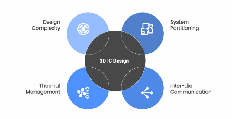
Designing a 3D integrated circuit involves much more than just stacking chips. Here are the main aspects engineers must master:
1. Partitioning the System
Partitioning is a critical first step. Engineers decide how the system is split across dies, balancing performance, power, and thermal considerations. Common partitioning strategies include functional (logic vs memory) or process-based (analog vs digital) approaches.
2. Inter-die Communication
To ensure seamless communication between dies, designers employ:
- Through-Silicon Vias (TSVs): Vertical connections through wafers.
- Micro-bumps and interposers: Used for 2.5D integration or redistribution layers.
- High-bandwidth die-to-die interfaces: Such as UCIe, Intel EMIB, or AMD Infinity Fabric.
3. Thermal Management
With multiple active dies stacked together, hotspots can become a serious issue. Thermal-aware floorplanning, advanced materials (e.g., diamond or graphene-based heat spreaders), and active cooling are essential.
4. Design and Verification Complexity
Multi-die design introduces complex physical design constraints, signal integrity challenges, and verification difficulties. Engineers rely on enhanced VLSI design tools that support 3D-aware modeling and parasitic extraction.
Packaging Technologies Enabling Multi‑Die Integration
The rise of multi-die systems has driven packaging innovation. The key enablers include:
- 2.5D ICs: Dies placed side-by-side on an interposer (silicon or organic substrate).
- Fan-out wafer-level packaging (FOWLP): Allows more I/O with lower parasitics.
- 3D ICs with TSVs: Full vertical integration for tight coupling and space efficiency.
- Advanced SoIC (System-on-Integrated-Chips): Used by TSMC to deliver ultra-high-density packaging.
Each approach has trade-offs in performance, cost, and manufacturing complexity. Choosing the right packaging method depends on the application and design priorities.
3D-ICs: Enabling the Next Generation of High-Density Integration
EDA and Simulation Tools for 3D ICs
EDA tool vendors have begun adapting their solutions for multi-die design. Modern tools must offer:
- 3D-aware physical design and placement tools
- Multi-die co-simulation environments
- Thermal and stress analysis modules
- Advanced test planning and yield analysis
Simulation and emulation must span both logic and package levels, enabling early detection of integration and reliability issues.
Test and Validation in 3D ICs
Testing is perhaps the most challenging phase of multi-die IC development. Standard scan-based testing becomes less effective due to limited probe access and multiple interfaces.
Best practices include:
- Pre-bond and post-bond testing of individual dies
- Built-in self-test (BIST) and Design-for-Testability (DfT) insertion
- Boundary scan techniques for inter-die I/Os
- System-level validation post-assembly
Given the high complexity, chip design teams must embed test strategies early in the lifecycle.
Real-World Applications of 3D IC Design
Multi-die architectures are already making an impact in production environments. Notable applications include:
- AI accelerators (e.g., AMD’s Instinct MI300 with multiple stacked dies)
- Mobile SoCs integrating modem, CPU, GPU, and memory
- High-end FPGAs with stacked interconnects and reconfigurable tiles
- Data center chips using chiplets for compute and memory separation
These designs demonstrate that the future of silicon is no longer flat; it’s three-dimensional.
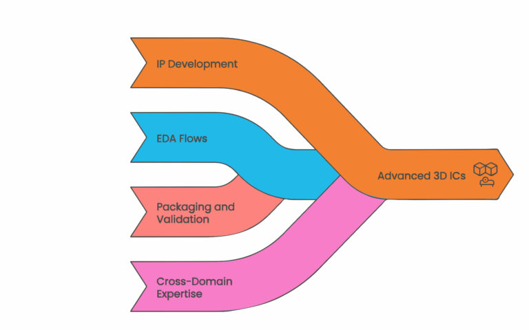
Leading chip design companies are no longer just designing chips; they’re building complete systems using advanced integration techniques. These companies are investing heavily in:
- IP development for high-speed interconnects
- Multi-die-aware EDA flows
- In-house packaging and validation labs
- Cross-domain expertise in logic, memory, analog, and RF
They are also forging close partnerships with foundries and OSATs (outsourced semiconductor assembly and test providers) to ensure manufacturability and yield optimization.
Tessolve: Accelerating Next-Gen Semiconductor Design
At Tessolve, we understand the complexity and promise of multi-die architectures. As a leading silicon and systems engineering company, we offer end-to-end solutions that span:
- Full-stack chip design, from architecture to RTL to GDSII
- Advanced VLSI design methodologies for both SoC and chiplet-based systems
- Expertise in test engineering, ATE validation, and post-silicon bring-up
- Packaging co-design and thermal modeling services
- Turnkey solutions across automotive, industrial, AI, and communications markets
Our customers trust us not just for design execution but for system-level innovation. With a global talent pool and state-of-the-art infrastructure, Tessolve is at the forefront of enabling the next generation of multi-die and 3D IC products.
Low-Power SoC Chip Design: Strategies for Mobile and IoT Devices
Conclusion: Embracing the 3D Future
The leap from traditional SoC to multi-die architecture isn’t just an evolution; it’s a revolution. As performance demands escalate and physical limits of silicon become more pronounced, 3D IC design offers a roadmap for sustained innovation.
Success in this domain depends on mastering heterogeneous integration, packaging, testing, and simulation. Whether you’re part of an emerging startup or one of the world’s leading chip design companies, adopting 3D methodologies is no longer optional; it’s essential. And with Tessolve at the helm, the path to a 3D-enabled future is not only achievable; it’s already underway.