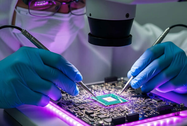

As semiconductor geometries shrink to 5nm, 3nm, and emerging sub-2nm technologies, the industry faces a host of fresh testing challenges. Shrinking transistors, increased variability, new packaging styles, and rising system complexity all conspire to make validation harder, slower, and costlier. The growing adoption of AI processors, chiplet-based architectures, advanced packaging, and high-bandwidth memory (HBM) has further increased the complexity of semiconductor testing. For teams responsible for bringing chips from design to production, mastering these hurdles is essential. In this post, we’ll walk through the principal obstacles and practical strategies that modern semiconductor testing teams use to keep pace, with a focus on pragmatic steps that semiconductor test engineers and broader test engineering organizations can adopt.
Why Advanced Nodes Break Old Assumptions
At 5nm and smaller, physical effects that were previously second-order become dominant. Process variability, quantum effects, and interconnect resistance create unpredictable behavior across lots and within wafers. Power density rises while the margin shrinks, making thermal behaviors and noise coupling more severe. The widespread adoption of Gate-All-Around (GAA) transistors, backside power delivery, and advanced EUV manufacturing further increases process complexity and demands more sophisticated testing methodologies. These changes force test engineering teams to rethink both what they measure and how they measure it.
For the semiconductor test engineer, this means test programs must grow smarter: richer stimulus, higher-resolution measurements, and more context-aware algorithms that can separate benign variability from actual defects. In short, standard production test recipes are often no longer sufficient for robust semiconductor testing at scale.
Key Technical Challenges
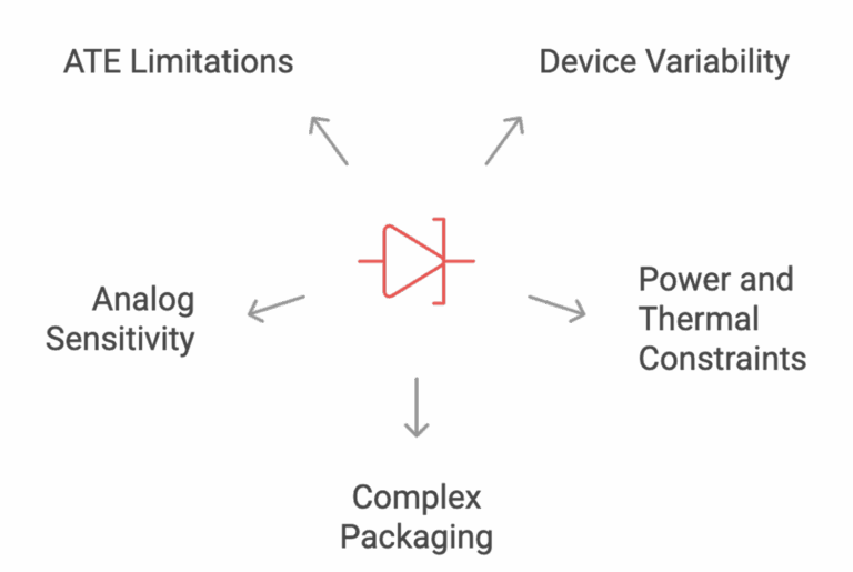
- Device variability and margin erosion: Smaller dimensions increase parameter spreads, requiring finer-grained AI-assisted statistical test methods and per-die adaptive limits to avoid mistaking yield loss for field risk.
- Power and thermal constraints: Higher power density means devices heat up during stress testing, changing characteristics. Thermal-aware test flows and on-chip temperature sensing become essential for realistic characterization and reliable manufacturing tests.
- Complex packaging and 3D integration: Chiplets, 2.5D/3D packaging, hybrid bonding, glass substrates, and heterogeneous integration add interconnect layers and new failure modes.
- Analog and mixed-signal sensitivity: With less margin, small analog errors can cause functional failures. The semiconductor test engineer must design precision measurements and carefully control test environments. High-speed SerDes (112G/224G), HBM interfaces, and advanced RF blocks require even greater measurement precision during validation.
- ATE and probe limitations: Modern ATE platforms increasingly support AI-assisted diagnostics, high-speed SerDes testing, and multi-die validation for advanced semiconductor devices. Upgrading hardware and co-optimizing test programs with ATE capabilities are common requirements for modern test engineering groups.
Overcoming Advanced-Node Testing Challenges: Key Strategies
The Future of Test Engineering in the Semiconductor Industry
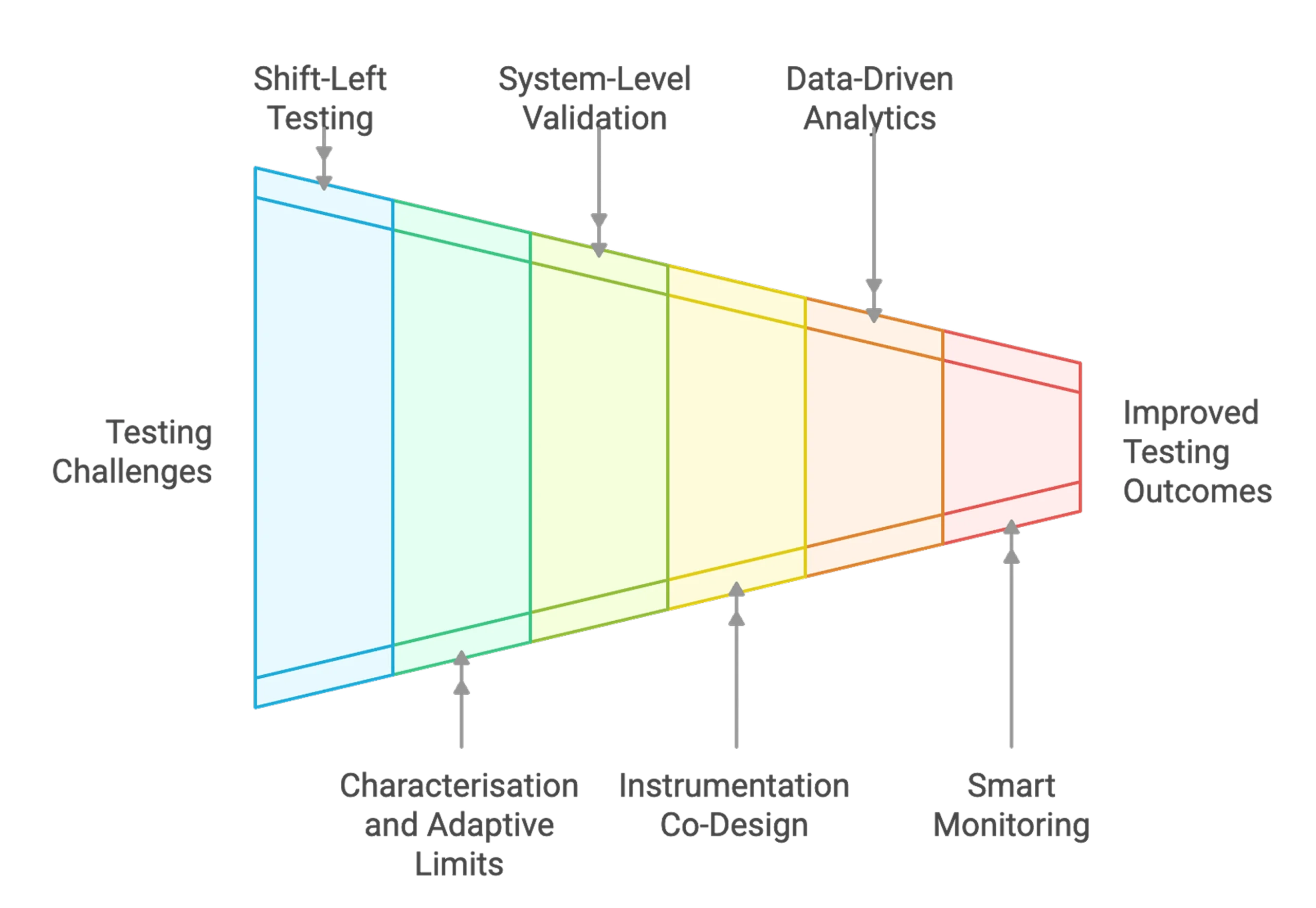
- Shift-left testing and earlier validation: To reduce late surprises, integrate testing earlier in the flow. Silicon-aware simulation, AI-assisted verification, digital twins, DFT (design-for-test) visibility, and early silicon bring feedback to designers sooner. When test engineering teams collaborate with design and DFT early, they can influence scan insertion, boundary-scan hooks, and observability for critical nodes, which simplifies later silicon debug and semiconductor testing coverage.
- Invest in characterization and adaptive limits: For transistors at 5nm and smaller, a one-size-fits-all approach to limits is inadequate. Instead, it’s essential to conduct thorough characterization across different process corners, temperatures, and voltage levels to support adaptive limit methodologies. Semiconductor test engineers should develop machine-learning-assisted statistical models, such as per-lot or per-wafer models, to help distinguish shifts caused by the manufacturing process from actual defects. This approach will improve both yield and field quality.
- Embrace system-level and mixed-signal validation: Advanced-node chips rarely operate alone. SLT (system-level test), hardware-in-the-loop setups, and real-application workloads will reveal interactions that simple functional patterns miss. A cohesive test engineering approach incorporates system-level scenarios into final acceptance tests and correlates system failures back to device-level metrics to close the loop on debug.
- Improve instrumentation and ATE co-design: To measure subtle effects at 5nm, both the ATE and probe infrastructure need upgrades: better thermal control, faster timing engines, and lower-noise analog front ends. The semiconductor test engineer should partner with ATE vendors and in-house hardware teams to co-design fixtures and handlers that preserve signal integrity during semiconductor testing.
- Use data-driven analytics and AI for yield learning: High-volume data from characterization, wafer maps, and in-line monitors is a goldmine. Modern test engineering groups apply statistical learning and anomaly detection to cluster failure modes, find latent correlations, and prioritize root-cause investigations. Automated triage reduces manual debugging time and accelerates corrective actions.
- Integrate Smart Monitoring and Contingent Extended Testing: To balance yield protection with deeper process insights, product and test engineers can incorporate targeted monitoring tests into the Automated Test Equipment (ATE) program. These tests do not impact production yield but offer valuable visibility into device behavior. Additionally, contingent extended tests can be triggered selectively when critical datasheet parameters fail. These controlled tests help capture data on process variations and device anomalies without causing systemic yield loss.
The key is to implement monitoring and extended routines wisely by limiting their scope, frequency, and duration, ensuring that the test time overhead remains manageable. Once process and device performance stabilize, these additional routines can be phased out, optimizing throughput without sacrificing valuable insights.
- Strengthen failure analysis and feedback loops: When a new failure mode appears, rapid failure analysis (FA), from electrical debug to package delidding and imaging, is critical. Close collaboration between FA labs and semiconductor test engineer teams ensures that lessons learned feed design and process changes quickly, shortening cycles and minimizing repeated yield loss.
Innovations in Test Engineering: Advanced Design-for-Test (DFT) Techniques for Modern ICs
People and Process: Training and Cross-functional Teams
At nodes this advanced, success is not just technical; it’s organizational. Cross-functional teams comprising design, DFT, PTE, and FA experts who collaborate closely minimize handoff delays. Investing in skill development for test engineering and hiring seasoned semiconductor test engineer talent who understand both silicon and system behavior pays off quickly.
Cost vs. Time-to-market Tradeoffs
Aggressive test coverage and characterization increase up-front cost and time, but uncontrolled escapes or repeat respins are far more expensive. Smart tradeoffs targeted stress tests, risk-based sampling, and adaptive test compression to help balance cost, quality, and schedule.
Roadmap: Where Teams Should Invest Next
- Support AI accelerators, chiplets, and advanced packaging.
- Invest in AI-driven yield analytics and predictive failure analysis.
- Expand validation for UCIe and heterogeneous multi-die systems.
- Adopt adaptive test limits and per-die intelligence to avoid unnecessary overkill.
- Build stronger partnerships with packaging and process teams to anticipate integration risks.
Role of Test Engineering in the Semiconductor Industry
Tessolve: Partnering to Solve Advanced-node Test Challenges
As semiconductor technologies advance to 5nm, 3nm, and the emerging 2nm era, test engineering has become a critical factor in ensuring product quality, yield, and reliability. Tessolve provides end-to-end test engineering services that help semiconductor companies address the growing complexity of advanced-node devices. Its capabilities include ATE test program development, wafer sort, package test, characterization, system-level testing, post-silicon validation, reliability qualification, and failure analysis, enabling seamless support from silicon bring-up to high-volume manufacturing.
With expertise across AI processors, chiplet-based architectures, advanced packaging, high-bandwidth memory (HBM), automotive, networking, and data center applications, Tessolve delivers scalable testing solutions for next-generation semiconductor products. Backed by global engineering teams, advanced test laboratories, and deep semiconductor expertise, Tessolve helps customers reduce debug cycles, improve yield, accelerate time-to-market, and confidently validate complex silicon for advanced process nodes, including the emerging 2nm technology landscape.
Let’s Qualify Integrity of Your Product For Faster Releases
Frequently Asked Questions
1. What are the challenges of testing mixed-signal devices in high-volume production?
Mixed-signal testing requires precise measurements, noise control, and efficient validation to maintain accuracy without increasing production test time.
2. How can semiconductor companies improve test coverage without extending validation cycles?
Early DFT planning, AI-driven analytics, adaptive testing, and automated validation improve fault coverage while keeping validation cycles efficient.
3. How can manufacturers improve yield and reduce escape rates during semiconductor testing?
Manufacturers use adaptive test limits, statistical analytics, failure analysis, and system-level validation to improve yield and reduce defect escapes.
4. What are the common challenges in semiconductor wafer testing?
Wafer testing faces challenges like process variability, thermal effects, probe accuracy, and identifying defects before high-volume manufacturing begins.
5. Why are advanced process nodes like 5nm and 2nm more difficult to test?
Advanced nodes have higher transistor density, tighter margins, greater variability, and complex packaging, requiring more sophisticated semiconductor testing methods.