
Post-silicon validation is a critical step in semiconductor development, serving as the bridge between design verification and product launch. It ensures that chips perform reliably under real-world conditions. However, as devices become increasingly complex with multi-die packaging, AI accelerators, and advanced nodes, manual validation and traditional debugging methods are no longer sufficient.
To meet the growing need for speed and precision, the industry is now pivoting towards automation and intelligent infrastructures for high-speed debug and traceability. This blog explores the evolution of post-silicon validation and the key trends shaping its future.
Why AI in IC Test & Product Engineering?
Modern SoCs and multi-die systems house billions of transistors and complex interconnects. Functional errors, power anomalies, or timing mismatches can emerge during real-world execution. Manual debugging becomes impractical when dealing with thousands of failure logs or intermittent bugs that are difficult to reproduce. This is where automated semiconductor testing plays a transformative role in delivering traceability, repeatability, and actionable insights.
More importantly, as markets demand faster time-to-market, any delays in post-silicon validation can create a ripple effect on product rollout, supply chains, and revenue.
Key Trends in Post-Silicon Validation and Debug Automation
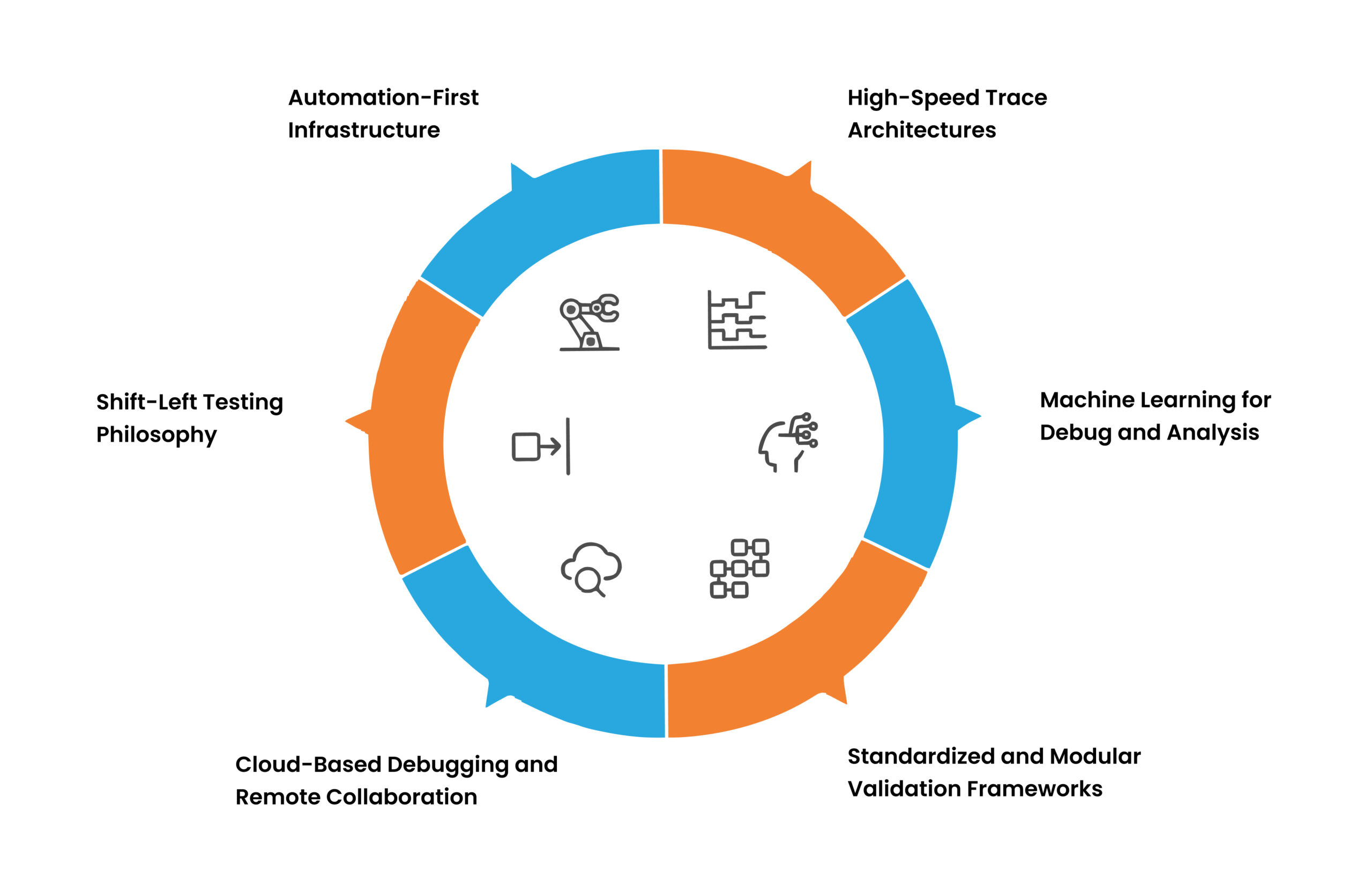
1. High-Speed Trace Architectures
To capture real-time chip behavior, designers are embedding on-chip trace logic like ARM’s CoreSight or Intel’s Trace Hub. These systems enable the non-intrusive recording of internal states, signals, and transactions, allowing for post-event analysis without pausing the system.
The latest trend focuses on optimizing trace bandwidth and compression. High-speed serial interfaces like PCIe and USB are being repurposed to extract trace data, and trace-aware logic design is enabling better observability across CPU, GPU, memory, and peripheral domains.
2. Machine Learning for Debug and Analysis
AI is making its mark in testing engineering. Machine learning models are used to analyze massive volumes of test data, identify patterns, and surface anomalies that might indicate functional or timing-related issues. Supervised models classify known issues, while unsupervised learning helps discover unknown bugs.
This significantly reduces the time validation engineers spend on manual log reviews and accelerates root cause identification.
3. Standardized and Modular Validation Frameworks
To streamline post-silicon processes, companies are turning to standardized frameworks based on IEEE 1687 (IJTAG) and IEEE 1149.1 (JTAG). These allow modular integration of test and debug logic, making it easier to reuse infrastructure across different chips and platforms.
Such frameworks are especially useful when working with outsourced engineering testing services, ensuring consistency across vendors and internal teams.
4. Cloud-Based Debugging and Remote Collaboration
Validation is becoming increasingly distributed. Engineers across geographies now collaborate via cloud platforms that host validation dashboards, waveform viewers, and debug logs. These systems enable remote access to test results, real-time monitoring, and centralized trace repositories.
Cloud also enables elastic compute resources, allowing for large-scale regression and stress testing in parallel, which speeds up feedback cycles.
5. Shift-Left Testing Philosophy
The “shift-left” approach, which pushes validation tasks earlier in the design cycle, is now being applied to post-silicon scenarios. By using hybrid emulation and simulation environments, engineers can validate, debug, trace flow, and verify system behavior before the first silicon arrives.
This proactive approach helps reduce post-silicon surprises and enhances test coverage during silicon bring-up.
6. Automation-First Infrastructure
Modern chip testing frameworks focus on eliminating manual steps, from stimulus generation to bug tracking. Automated test benches, programmable analyzers, and auto-triggered probes streamline validation workflows.
By combining automation with real-time feedback and integrated AI tools, validation teams can compress months of debug effort into weeks.
Innovations in Test Engineering: Advanced Design-for-Test (DFT) Techniques for Modern ICs
Challenges in Automation of Post-Silicon Validation
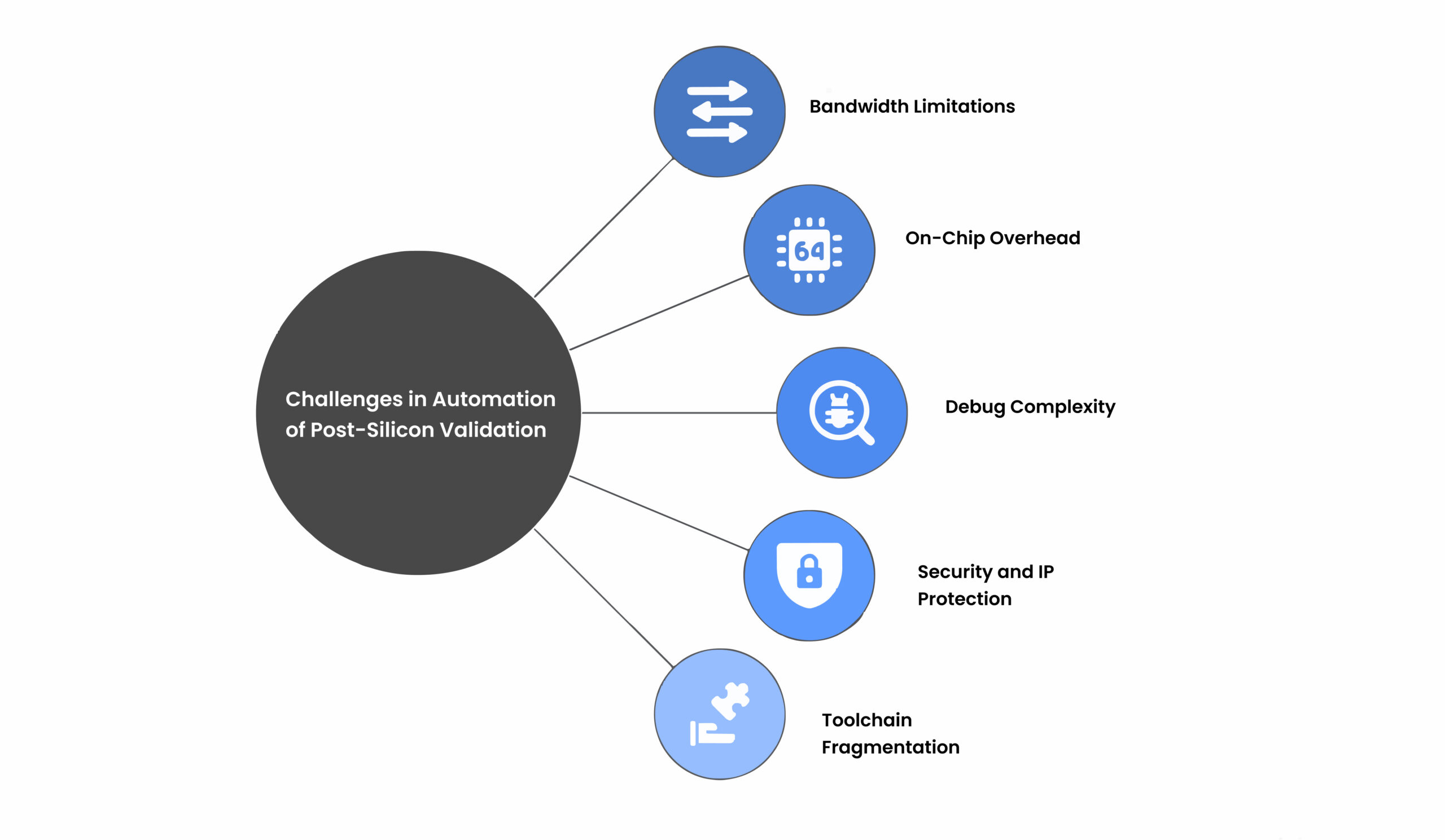
Despite major advancements, automation in post-silicon validation faces several hurdles:
- Bandwidth Limitations: Even with high-speed interfaces, the volume of trace data can overwhelm systems. Efficient compression and filtering are necessary.
- On-Chip Overhead: Debug and trace logic consume valuable silicon area and power. Designers must balance observability with cost and performance trade-offs.
- Debug Complexity: Non-deterministic issues caused by concurrency or timing anomalies are still difficult to pinpoint, even with automated workflows.
- Security and IP Protection: Moving sensitive debug data to the cloud raises concerns over IP leakage and data privacy.
- Toolchain Fragmentation: Lack of interoperability between proprietary debug tools and frameworks slows down integration and collaboration efforts.
Addressing these challenges requires collaboration across design, validation, and tooling teams, as well as investment in future-ready infrastructure.
Tessolve: Accelerating Post-Silicon Success
At Tessolve, we understand the critical role automation and precision play in modern post-silicon validation. As a global leader in engineering testing services, our mission is to support semiconductor companies in launching robust, high-performance products—faster.
Here’s how we make a difference:
- Complete Validation Ecosystem: From chip testing and bring-up to high-speed debug and trace, we offer end-to-end validation services.
- AI & Automation Integration: Our test flows leverage ML-driven analytics, automated regression setups, and remote lab access for rapid feedback.
- Advanced Lab Infrastructure: Equipped with the latest tools and trace technologies, our labs are ready for complex SoCs, automotive ICs, and AI accelerators.
With Tessolve, you gain a partner that not only understands the technical depth of testing engineering but also delivers the agility and scale required in today’s competitive semiconductor landscape.
The Future of Test Engineering: How Automation is Changing the Game
Conclusion: Automation is the Future of Validation
The evolution of post-silicon validation is driven by necessity, as chips have become more complex, timelines tighter, and quality demands higher than ever. Relying on manual debugging or fragmented workflows is no longer a sustainable approach. Automation, AI, and trace-first architectures are not just innovations; they are strategic enablers.
By investing in smarter semiconductor testing strategies and leveraging modern tools, organizations can reduce validation cycles, improve product quality, and accelerate time-to-market. Whether you’re a startup building your first SoC or an enterprise launching multi-die systems, automated post-silicon validation is your gateway to engineering excellence.