Innovation in 5G technology in the automotive application industry is accelerating with IoT innovations, deployment of high-speed networks, and in-vehicle technologies. However, some crucial reasons exist for developing these technologies, such as the 5G PCB design board and hardware design. Nowadays, the focus has shifted toward “Software-Defined Silicon,” where CAD tools must account for the specific application workloads, like Generative AI or autonomous driving, during the earliest stages of physical design.
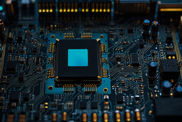
In the world of electronics, the importance of VLSI (Very Large Scale Integration) technology cannot be overstated. VLSI physical design plays a crucial role in creating integrated chip designs that power modern devices. It involves intricate processes and algorithms that ensure the optimal performance and functionality of integrated circuits. In this blog, we will explore VLSI CAD (Computer-Aided Design) and delve deep into :
- VLSI CAD and Its Significance
- VLSI Physical Design Flow
- Current Trends in VLSI CAD
- Why Tessolve?
Understanding VLSI CAD and Its Significance
VLSI CAD came as a powerful technology that empowers engineers to create highly complex and efficient integrated chip designs, revolutionizing the development of VLSI solutions. Using CAD tools, engineers can intelligently optimize every facet of the design process, including the strategic placement and routing of components on the chip.
Moreover, VLSI CAD enables engineers to achieve remarkable advancements in reducing power consumption. With the shift to “Backside Power Delivery” (BPD) at 2nm nodes, CAD tools are now essential for managing vertical power distribution and reducing voltage drop (IR drop) across the die.
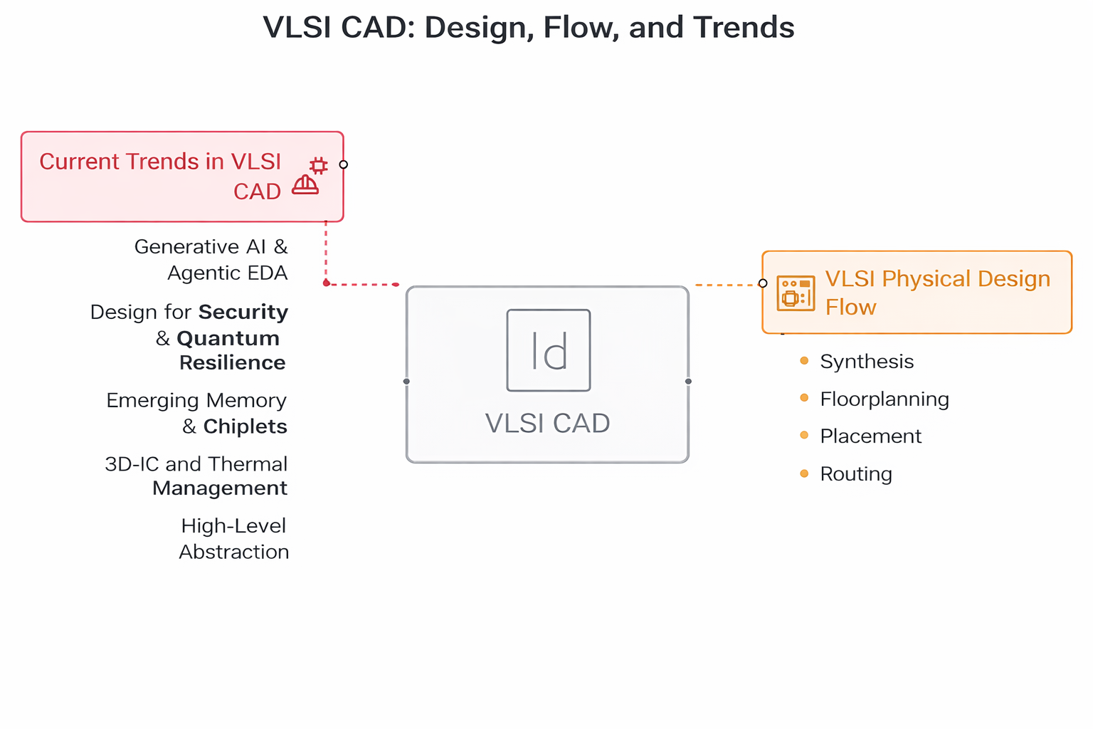
VLSI Physical Design Flow
The VLSI physical design flow encompasses a set of steps that engineers follow to transform a concept into an actual integrated chip design. This flow involves multiple stages, including synthesis, floorplanning, placement, routing, and verification. Each stage has its respective algorithms and tools that aid in achieving a successful design.
Synthesis
The synthesis stage involves transforming an RTL (Register Transfer Level) design into a gate-level representation. Modern synthesis engines now perform “Predictive Placement” to forecast routing congestion before the layout even begins.
Floorplanning
Floorplanning is the initial step that determines the overall chip layout. By placing different functional blocks, memories, and I/O pins on the chip, engineers ensure efficient communication and minimize interference between components.
Placement
Placement involves determining the positions of all components. Advanced algorithms now use “Machine Learning-based timing prediction” to place cells in a way that minimizes total wirelength and maximizes signal integrity for high-speed 224G SerDes interfaces.
Routing
Routing is the process of connecting the components on the chip through metal tracks, ensuring efficient communication and signal integrity. Algorithms optimize the routing based on factors like congestion, wirelength, and electrical constraints.
Discovering Current Trends in VLSI CAD
As technology advances, new trends emerge in the VLSI CAD industry that can impact the design and verification process. Here are some of the current trends in VLSI CAD of 2026:
- Generative AI & Agentic EDA: CAD tools now feature “Agentic AI” co-pilots that can autonomously write ECO (Engineering Change Order) scripts and fix timing violations without human intervention.
- Design for Security & Quantum Resilience: With cybersecurity becoming a national priority, CAD tools now include “Post-Quantum Cryptography” (PQC) IP blocks and “Hardware Trojan” detection algorithms built directly into the verification suite.
- Emerging Memory & Chiplets: As traditional memory reaches its limits, MRAM (Magnetic RAM) and RRAM (Resistive RAM) are being integrated. CAD tools are now optimized for “Chiplet-based architectures,” using the UCIe standard to verify communication across multiple dies on a single interposer.
- 3D-IC and Thermal Management: Three-dimensional integrated circuits (3D-ICs) are now the standard for AI accelerators. 2026 CAD workflows feature “Multi-Physics Simulation,” analyzing thermal, mechanical stress, and electrical parameters simultaneously to ensure 3D-stacked chips don’t overheat.
- High-Level Abstraction (HLS 2.0): HLS tools now allow designers to use Python and C++ to generate hardware directly, enabling “Software-Hardware Co-design” where the chip architecture is optimized for a specific AI model’s weights and data flow.
Increased Importance of VLSI Design Ecosystem in India for Worldwide Semiconductor Industry
Why Tessolve?
The United States has been a hub for VLSI design innovation, with numerous companies and research institutions contributing to the advancement of VLSI technology. Many leading VLSI solutions and CAD tools have originated from the USA, making it an influential player in the global VLSI industry. Tessolve has established itself as a leading VLSI design in USA, and several factors contribute to its reputation as the best in the industry. First and foremost, Tessolve boasts highly skilled and experienced engineers with VLSI design expertise. This expertise allows us to craft innovative and efficient solutions for complex design challenges. We believe in the holistic approach to incorporate the latest technologies, tools, and methodologies to stay ahead of the rapidly evolving semiconductor landscape.
Conclusion
VLSI CAD has revolutionized the world of integrated chip design, enabling engineers to create complex and efficient designs with superior performance. By utilizing VLSI CAD tools and following the VLSI physical design flow, engineers can design cutting-edge integrated chip designs.
If you are also looking for semiconductor solutions, you can rely on Tessolve. As the leading VLSI engineering partner for manufacturers and semiconductor companies, we are dedicated to constantly refining our ASIC design capabilities. From the initial concept to creating flawless design specifications and faster tape-outs, we leave no stone unturned in delivering superior results.
Choose Wisely, Choose Tessolve !!
Frequently Asked Questions
1.What is “Agentic EDA” in modern VLSI design??
It refers to AI agents that autonomously navigate CAD tools to optimize chips, fix bugs, and achieve timing closure with minimal human input.
2. How does 3D-IC design change the CAD workflow?
It requires “Multi-Physics” tools that simulate heat, stress, and electrical signals across multiple stacked dies simultaneously.
3. Why is “Design for Security” important in 2026?
To protect against hardware hacking and ensure chips are resilient against future quantum-computing decryption threats.
4. What is the role of RRAM and MRAM in 2026 chip design?
These are emerging non-volatile memories that offer much higher density and lower power than traditional Flash, ideal for Edge-AI sensors.