Both consumers and businesses demand more innovative products with advanced technologies and abilities. Therefore, there is a rapid progression and development in electronic technology. Printed Circuit Boards, or PCBs, are one of the most necessary components of every electronic device in today’s world. Launching any technology involves PCBs, and PCBs should adapt to the rising needs of the technologically advanced world. Electronic Device should keep these trends in mind when designing their products.
Let us know in detail what PCBs are before going through the PCB trends.
What are PCBs?
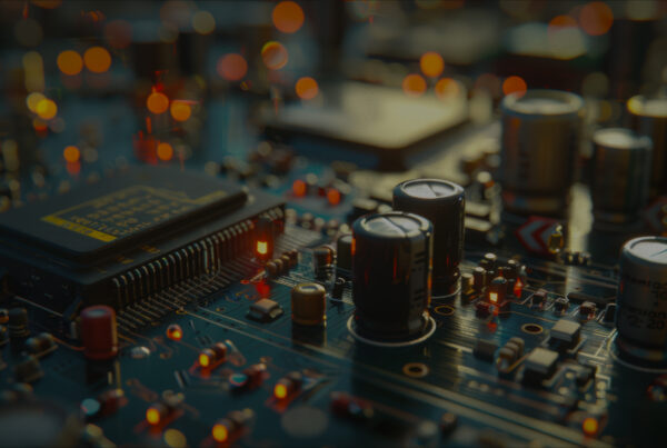
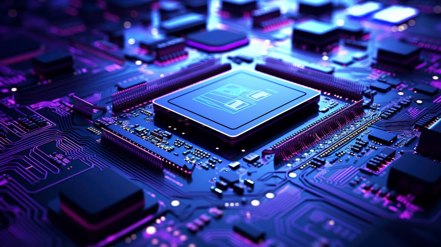
A Printed Circuit Board facilitates the operation and functioning of anything electronic. These minuscule components are the most significant elements of any technology ever invented. A PCB looks like a flat plate having a pattern of conducting material and parts.
Common Uses of PCBs
Any device with an electronic component requires a minimum of one printed circuit board, meaning that PCBs are essential to every industry. Some of the most typical industry usages of PCBs are :
- Industrial – Manufacturing equipment, assembly machines, and equipment for measuring temperature and pressure need PCBs.
- Healthcare – Scanning equipment, research tools such as compressors, microscopes and control systems, blood glucose monitors, and blood pressure and heart rate monitors require PCBs.
- Automotive – PCBs are in control systems, car sensors, and navigation systems.
- Oil Industry – Monitoring and downhole sensors use PCBs.
- Lighting – Light-emitting diodes also have PCBs.
- Military Aerospace – Power supplies, flight systems, hardware, and monitoring and communication equipment cannot function without PCBs.
Current PCB Trends followed by PCB Manufacturers.
The PCB industry is one of the fastest-growing industries, and studies show that the total worth of the sector will be nearly $76 billion by the end of 2025. The newest trends and manufacturing processes are constantly changing to make PCBs satisfy the rising demands.
Let us look at the latest PCB trends :
High-Speed PCBs
In the era of 5G, the need for Speed has greater impact on the PCB design. To meet this growing demand for speed, Hardware design engineers must ensure that PCB Design, Materials and Manufacturing improves the Signal Integrity of the design. PCB designers should understand the impact of Dielectric material, vias, trace length, cross talk, impedance discontinuities on the Signal Integrity and design their PCB. PCB Designers should also make use of new features in EDA tools that helps design right the first time.
High-Density Interconnect PCBs
There are rapid developments in automation in almost every industrial landscape. New advancements are common in every sector, from military communications and aerospace applications to medical diagnostics tools and wearable technology. Therefore, the need arises for HDI PCBs. High-density interconnects (HDI) PCBs are smaller and lightweight than other PCBs and offer high-speed and reliable signals. These PCBs designed by hardware design engineers provide a proper circuit route with different routing options.
HDI PCBs have improved wiring density and lower smaller trace widths, which allows engineers to stuff more power and functionality into little space. They also decrease the requirement for layering, reducing production expenses. Thus, HDI PCBs are becoming more significant in the latest devices and technology.
Internet of Things (IoT)
Communication is necessary for all products, and it has been made possible through IoT in various ways. The Internet of Things defines the network of physical objects infused with software, sensors, and other technologies for exchanging and transferring data from one device or system to another over the internet. IoT parts are included while manufacturing PCBs, and any IoT gadget requires power, wireless connectivity, and sensors. To satisfy these criteria, it is essential to change the design of PCBs. For instance, smartwatches are getting smaller; thus, they need to fit more functionality within a smaller space. Users also expect the devices to run for a long time, so the PCB designs should have long battery life.
Thus, PCB designers embrace the challenges of meeting all electrical requirements and manufacturing constraints with the ever-shrinking devices.
High Power Boards
The need for high power boards is increasing endlessly. This is due to the growth of electric devices, which demand high voltage boards like 48V and more elevated. There is also a great demand for solar panels that function at 24V or 28V.
Commercial Off-The-Shelf Solutions
These PCBs, known as COTS, have modules, components, and boards. COTS parts can easily be installed into present systems. COTS is extensively used in aerospace sector. Current space development solutions use PCB COTS developed by hardware design engineers to minimize the expenses of significant initiatives and ensure safety, superior quality, and quick completion of projects.
Biodegradable PCBs
Electronic waste problems create a global issue, and biodegradable PCBs are manufactured to minimize these issues. Previously, the problem of disposing of PCBs started with environmental issues as they had chemicals in them and were also undegradable. These issues were resolved when biodegradable PCBs came to be manufactured. Further, the metals such as gold, silver, palladium, gallium, and tantalum are extracted from the chips and reused.
Flex PCBs
A single board manages different functions; thus, a flexible layout is needed for PCB functionality. Flex PCBs can resist harsh environments, such as dropping a phone by mistake to launching a missile. They also provide better reliability and capability and take up little space. Flex PCBs can tackle mode stress and transform it into the required size and shape. Their ability to flexibly attach to any component has resulted in the developing of various new medical instruments.
AI is undoubtedly one of the hottest technical directions of computational photography, and mobile photography is the application that benefits the most. The proportion of AI in machine vision is also becoming very significant in the photography direction and the automotive, industrial, security, and other markets. AI-specific processors or units are completely entering the image processing process.
Tessolve can design and deliver PCBs ranging from single-sided to multilayers, quick-turn samples to production orders, and small quantities to volume manufacture. We cater to all your complex needs.
Tessolve is one of the best professional printed circuit board design center with experienced Design Engineers and in-house Simulation and Mechanical Engineering team. Are you looking for the best-in-class PCB? Contact us right away!
For better assistance from our experienced engineers, email us today sales@tessolve.com.