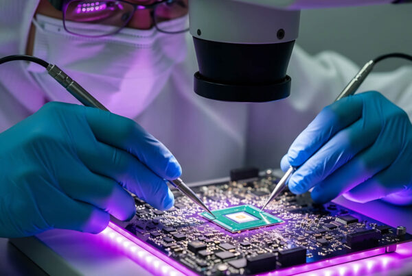
There is a widespread belief that hardware design and PCB design are the same thing. However, they are separate but complementary phases of electronic product development. Hardware design defines the system architecture, selects components, and ensures overall functionality. On the other hand, PCB design converts that architecture into a physical board layout for manufacturing. These two processes differ in a few ways, including scope, skill set, level of abstraction, design workflow, and tools used.
As modern electronic systems incorporate AI accelerators, high-speed interfaces, advanced packaging, and chiplet-based architectures, understanding the distinction between hardware and PCB design has become even more important for successful product development and cross-functional engineering collaboration. Learn more about the key differences between PCB and Hardware design here.
What is Hardware Design?
Hardware design is an engineering practice that specifies how electronic systems, circuits, and devices operate. Tessolve’s hardware design extends from recording system-level intent to the delivery of manufacturable, high-reliability hardware.
The most crucial elements of hardware design are:
- System architecture & functional planning; specifying interfaces, high-level structure, and important performance constraints
- Component library & selection services; managing symbols, footprints, and checking part feasibility
- Schematic capture & circuit design; converting architecture into electrical connections and board-level design.
- Simulation & analysis; signal integrity (SI), power integrity (PI), thermal, EMI/EMC, and high-speed interface validation for modern electronic systems.
- Mechanical & electro-mechanical assembly; creating enclosures while optimizing structural, thermal, and manufacturability requirements.
- Design-for-manufacturability (DFM) & turnkey delivery; utilizing in-house CAM checks, partner fabs, and assembly services for production volumes
Modern hardware design also considers high-speed connectivity, embedded AI processing, security, scalability, and long-term product reliability before detailed PCB implementation begins.
Channel Modeling and Simulation for High-Speed PCB Design Verification
What is PCB Design?
PCB design is the technical subset of hardware engineering responsible for converting schematic logic to a physical, manufacturable board. Tessolve’s PCB design services focus on reliability, manufacturability, and compliance under actual conditions.
Major aspects of PCB design are:
- Component placement & layout optimization; placing parts to optimize signal paths, heat, and routing simplicity
- Trace routing & signal integrity; ensuring controlled impedance, minimizing crosstalk, and supporting high-speed interfaces such as PCIe, DDR, USB, and Ethernet.
- Power and ground strategy; using ground/power planes, decoupling schemes, and clean return paths
- Multilayer stack-up & material design; selecting appropriate materials for high-speed, RF, and high-frequency applications.
- Thermal management; optimizing heat dissipation using thermal vias, copper balancing, and heatsink integration.
- DFM / DFA & CAM validation; running VALOR (or equivalent) checks, following IPC guidelines, and assembling for optimization
In a delivery model, PCB hardware design is at the center of making functional electronics a reality. It is augmented with schematic capture, library services, simulation, and mechanical design to be an end-to-end turnkey hardware solution. Industry tools such as Allegro, Xpedition, Altium Designer, KiCAD, and others are used by their teams to assist in complex, high-speed board design.
Modern PCB design also leverages advanced SI/PI simulation, 3D visualization, AI-assisted routing optimization, and digital twin technologies alongside tools such as Allegro, Xpedition, Altium Designer, and KiCad.
Best Practices in High-Density Interconnect (HDI) PCB Design for Complex Products
Differences Between Hardware Design and PCB Design
Hardware Design vs PCB Design involves understanding how electronic systems are conceptualized and implemented. While hardware design focuses on the overall functionality and architecture of a system, PCB design deals with the physical layout and interconnection of components on a board.
| Category | PCB Design | Hardware Design |
| Focus and Goals | PCB hardware design focuses on creating a layout for the interconnection of electronic components on a PCB. It allows companies to optimize the placement of electronic components, power distribution, and routing of signal traces to ensure the device’s functioning. PCB design converts the hardware architecture into a manufacturable layout while optimizing signal integrity, power integrity, thermal performance, EMC compliance, and production readiness. |
Hardware design helps companies conceptualize and define the overall architecture of an electronic system for improved functionality. It aids in selecting appropriate components to improve system behavior and establishes the interactions between different hardware modules, meeting device functional requirements. With the help of hardware design, companies can create a comprehensive electronic system tailored to their specific needs, including size, power, cost, and performance. |
| Skill Sets and Expertise Requirement |
To create a PCB layout and ensure proper functionality and manufacturability, a PCB design engineer must understand electronics. They should know various PCB design software, as companies use different software according to their specific needs. PCB designers must understand PCB design and development along with its manufacturing process and concepts like thermal considerations, impedance matching, Signal and Power integrity, and EMI/EMC mitigation techniques. Designers should also understand high-speed interfaces, advanced stack-up design, SI/PI analysis, thermal optimization, and modern PCB manufacturing technologies. |
On the other hand, a hardware designer must have a broad understanding of electronics to conceptualize, create, and refine the architecture of the electronic device. They must also be well-trained in design principles to optimize and analyze the complex electronics system. They should also understand system architecture, embedded processing, power management, high-speed interfaces, and hardware-software co-design principles. |
| Design Tools and Software |
To create a reliable, efficient, and cost-effective board design, a PCB design engineer must have a thorough knowledge of PCB design software and tools. It helps designers to create high-speed PCB layouts, manage constraints, perform SI/PI analysis, and generate manufacturing-ready outputs. |
To work on hardware design and development, hardware designers must understand various tools to create electronic circuit diagrams.
|
Hardware Turnkey Flow
- Schematic Development: Incorporates DUT information, tester configuration, channel mapping, and circuits involved.
- Library Creation & BOM Scrubbing: Ensures accurate component management and up-to-date libraries.
- Mechanical Data Import: Includes tester templates, handler docking plates, stiffener inlays, and RF brackets.
- Placement & Critical Signal Routing: Performs single-site placement, followed by multi-site designs; a preliminary BOM is released.
- Stack-Up Optimization: Optimizes stack-up for high-speed interfaces, signal integrity, thermal performance, manufacturability, and cost.
- Signal & Power Integrity Analysis: Performed throughout the design cycle using advanced simulation tools to validate SI, PI, EMI, and thermal performance.
- Routing: Efficient routing for faster turnaround without compromising quality.
- Final File Verification: Checks compliance with DFM and vendor design rules. Tessolve and other qualified vendors can contribute to PCB Fabrication & Assembly, including SEICA testing.
- Loadboard Diagnostics: Programs verify relays, active components, and passives.
Collaboration Between Hardware and PCB Designers
For a successful design, both PCB design engineers and hardware designers must be on the same page. They should collaborate from the initial stage to define the project’s requirements, goals, and constraints. The communication between them helps solve constraints, such as the size of the hardware board design, thermal considerations, power requirements, and any specific guidelines. Moreover, they must provide regular feedback to improve the final design.
Early collaboration also helps optimize component placement, high-speed routing, thermal performance, and manufacturability while reducing costly redesign cycles.
5G IoT & How It Is Significant for the Future of Connected Vehicles
Conclusion
Understanding the difference between hardware design and PCB design is essential for building reliable electronic products. As systems become more compact and incorporate AI, high-speed interfaces, and advanced semiconductor technologies, close collaboration between hardware and PCB teams is critical for achieving optimal performance, reliability, and manufacturability. At Tessolve, we provide end-to-end hardware engineering services, including hardware architecture, schematic capture, PCB layout, package engineering, mechanical engineering, SI/PI analysis, and manufacturing support to help customers accelerate product development with confidence.
Get in touch with us and get the right hardware design solution!
FAQ
1. What skills and tools are needed for PCB design vs hardware design?
Hardware design requires knowledge of circuits and system architecture, while PCB design needs expertise in CAD tools, routing, and layout optimization.
2. How does the interaction between PCB layout and mechanical enclosure design in electronics affect product performance
Proper coordination between PCB layout and mechanical enclosure design improves thermal performance, connector alignment, EMI control, manufacturability, and overall product reliability.
3. How do design revisions in hardware affect PCB design?
Any hardware change often requires PCB rework, making early validation and close collaboration critical to avoid costly iterations.
4. What is the difference between PCB design and PCB board design?
PCB design includes schematic capture, layout, routing, and validation, while PCB board design mainly focuses on the physical board structure and manufacturability.
5. Why is simulation important in hardware and PCB design?
Simulation software such as SPICE, SI/PI simulators, and 3D modeling identifies defects early, decreases rework, and ensures performance validation prior to physical prototyping, saving time and money.