The semiconductor industry has always been at the forefront of technological innovation, driving advancements in computing, communication, and countless other sectors. Test engineering plays a crucial role in ensuring the reliability and performance of semiconductor devices, and as technology evolves, so does the field of test engineering. The industry is moving toward “Test-as-a-Service” (TaaS) models and the widespread use of “Digital Twins” to simulate silicon behavior long before the first wafer is even sliced.
In this blog, we will explore the future of test engineering in the semiconductor industry, focusing on the future needs of different industries.
Introduction to Semiconductor Test Engineering
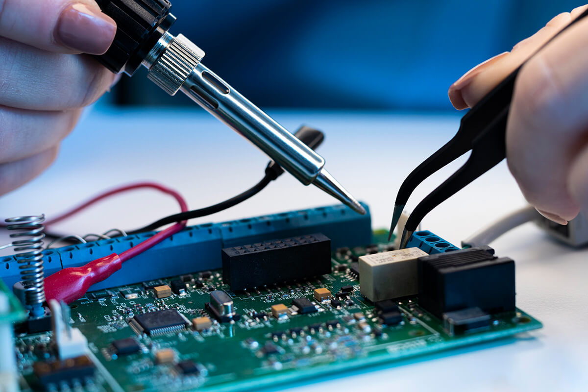
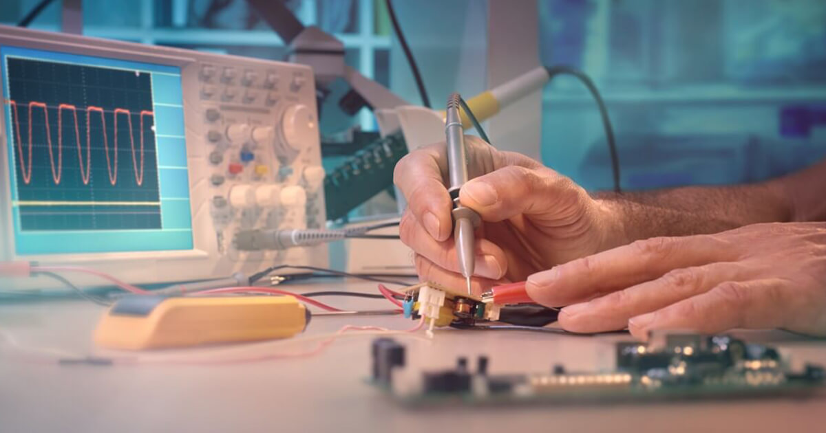
Semiconductor test engineering involves the validation and verification of integrated circuits (ICs) to ensure they meet quality and performance standards. Traditionally, engineers have used Automated Test Equipment (ATE) and specialized programs. However, as we hit the limits of Moore’s Law at the 2nm/1.6nm (A16) nodes, testing must now account for quantum-tunneling effects and thermal bottlenecks that were previously negligible.
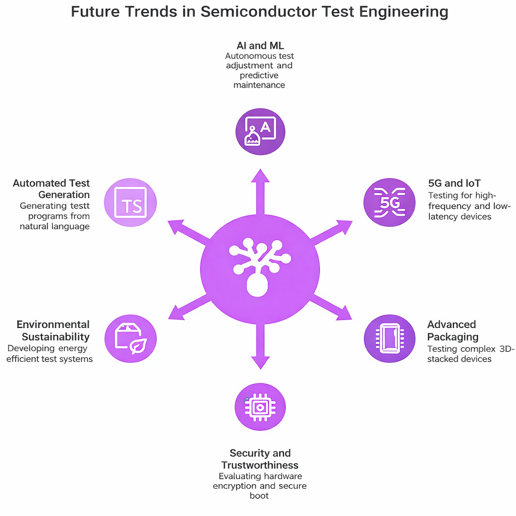
1. AI and Machine Learning in Test Engineering
Artificial intelligence (AI) and machine learning (ML) are revolutionizing many industries, and semiconductor test engineering is no exception. “Agentic AI” tools are being used to autonomously adjust test limits during high-volume production, maximizing yield without compromising safety. AI-powered test systems can analyze vast amounts of test data in real-time, making it possible to detect subtle defects or performance deviations that might be missed by traditional methods.
One of the most significant applications of AI in semiconductor test engineering is predictive maintenance. Machine learning algorithms can predict when ATE equipment is likely to fail, allowing for proactive maintenance to minimize downtime. Additionally, AI can optimize test patterns and reduce test times, leading to more efficient and cost-effective testing processes.
2. 5G and the Internet of Things (IoT)
The rollout of 5G networks and the proliferation of IoT devices have created new challenges for semiconductor test engineering. The focus has shifted toward 5G-Advanced and early 6G research, demanding testing for Terahertz (THz) frequencies and sub-millisecond latency. These technologies demand higher data rates, lower power consumption, and greater reliability. Test engineers are working to develop innovative test solutions that can meet these requirements.
One of the key technical challenges in testing 5G and IoT devices is ensuring that they can operate in diverse and real-world environments. Test engineers now use “Over-the-Air” (OTA) testing in anechoic chambers to simulate complex beamforming and spatial multiplexing scenarios found in urban environments. Advanced test systems are being developed to simulate these conditions accurately.
The Future of Connectivity: Exploring 5G Networks
3. Advanced Packaging Technologies
As semiconductor devices become smaller and more complex, advanced packaging technologies are becoming increasingly important. Techniques such as system-in-package (SiP) and 3D stacking enable multiple chips to be integrated into a single package, saving space and improving performance. However, these advanced packaging technologies pose unique challenges for test engineering.
Testing a 3D-stacked device is notoriously difficult, as many connections are buried inside vertical interconnects (TSVs). Test engineers must develop new strategies for testing devices with complex package structures. This includes developing specialized test sockets and fixtures that can access all the device’s connections. Innovation in “Micro-bump” probing and optical inspection allows for non-destructive testing of internal package layers, catching defects early in the manufacturing process.
4. Security and Trustworthiness
With the increasing integration of semiconductor devices into critical infrastructure and consumer products, security and trustworthiness have become paramount concerns. Test engineering now encompasses evaluating the security features of chips, such as hardware-based encryption and secure boot mechanisms.
One of the aspects of securing semiconductor devices is developing tests that can detect vulnerabilities and ensure that security features are functioning correctly. Test engineers are also working on methods to protect the integrity of the test process itself, ensuring that it cannot be compromised by malicious actors.
Environmental Considerations
Environmental sustainability is a growing concern in the semiconductor industry. Test engineering is not exempt from this trend. Test engineers are developing more energy-efficient test systems and exploring ways to reduce the environmental impact of semiconductor testing.
One approach is the development of low-power test methodologies. By 2026, “Adaptive Voltage Scaling” (AVS) during test execution ensures that the device under test consumes only the minimum power required, reducing the carbon footprint of massive test floors. Additionally, the recycling and responsible disposal of test equipment and materials are receiving increased attention.
5. Automated Test Generation and Debugging
The complexity of modern semiconductor devices makes test program development a challenging task. Large Action Models (LAMs) now allow engineers to generate entire C++ or Python-based test programs from natural language specifications. Automated test generation tools can analyze device specifications and automatically generate test programs, reducing development time and potential errors.
Furthermore, automated debugging tools are becoming essential in identifying the root causes of test failures quickly. By using “Knowledge Graphs” that link design intent to silicon results, these tools can pinpoint issues in complex multi-die systems in minutes rather than days.
6. Collaboration and Standardization
As the semiconductor industry becomes more global and interconnected, collaboration and standardization are critical aspects of test engineering. Test engineers are working together to establish common test standards and practices that can be applied across different regions and industries.
Standardization efforts are particularly important in ensuring interoperability between different test equipment and software platforms. This reduces compatibility issues and enhances the efficiency of semiconductor testing on a global scale.
Automated Test Equipment (ATE) Modernization: Enhancing Efficiency in Electronics Testing
Wrapping Up
The future of test engineering in the semiconductor industry is characterized by rapid technological advancements and evolving challenges. From harnessing the power of AI and ML to address complex testing scenarios to ensuring the security and environmental sustainability of test processes, test engineers are at the forefront of innovation. As the semiconductor industry continues to drive technological progress, test engineering will remain a critical component in ensuring the reliability and performance of semiconductor devices in the years to come.
At Tessolve, we are committed to providing cutting-edge Engineering & Testing Solutions and Engineering & Specialty Testing Services to meet the evolving needs of the semiconductor industry.
“Trust Tessolve to transform complex requirements into reliable Hardware Solutions.”
Frequently Asked Questions
1. What is the impact of 2nm manufacturing on test engineering?
It introduces massive process variation, requiring sophisticated statistical models to distinguish between “bad” chips and “slow but functional” ones.
2. How does AI reduce semiconductor test costs?
AI identifies redundant tests and removes them from programs, shortening test time per chip while maintaining 100% quality coverage.
3. How can semiconductor test solutions help reduce time-to-market for new semiconductor products?
Automated, AI-driven test solutions use predictive analytics and real-time data to catch defects early, streamlining validation and manufacturing cycles.
4. How do AI and new technologies impact semiconductor test sockets?
AI optimizes socket design for better signal integrity, while advanced packaging (SiP/FOWLP) requires specialized, high-durability sockets for 3D structures.
5. What do engineers use to test their designs of new technologies?
Engineers utilize Automated Test Equipment (ATE), high-bandwidth oscilloscopes, and AI-powered simulation tools to verify functional, electrical, and thermal performance.