
Semiconductor innovation is accelerating at an extraordinary pace, and with that speed comes a growing challenge in verifying increasingly complex chip designs. Functional verification has now become one of the most critical stages in the chip development lifecycle, often consuming a significant portion of engineering time and resources. As modern chips integrate billions of transistors and move toward advanced nodes like 2nm and beyond, traditional verification approaches that rely heavily on manual effort struggle to keep up.
The complexity further increases with the adoption of heterogeneous architectures, such as chiplets and advanced packaging technologies. To address these challenges, the semiconductor industry is rapidly embracing AI-driven verification tools alongside formal techniques. Together, these technologies help automate verification workflows, accelerate coverage closure, and enable engineering teams to deliver reliable silicon faster and more efficiently.
The Evolving Landscape of Semiconductor Designs and Chip Verification Process
Modern semiconductors with custom chip designs require robust verification to ensure functionality, performance, and reliability. The verification process involves rigorous testing, such as identifying defects and ensuring compliance with specifications, saving time and money.
These AI-powered tools help automate the generation of test cases and error identification, effectively reducing manual efforts. This integration enhances accuracy and efficiency and empowers engineers to focus on driving the semiconductor industry forward into the new era of designs and verification excellence. In modern semiconductor development, verification environments must also support extremely dense designs built on advanced nodes such as 2nm and sub-2nm processes, along with heterogeneous architectures like 3D-IC chiplets and high-bandwidth interfaces such as 224G SerDes.
How do AI and Formal Techniques Facilitate Chip Verification?
Chips evolve billions of transistors, sophisticated functionalities, and traditional verification methods struggle to keep pace. However, modern methods of chip verification involve various things, from virtual mode creation to RTL development to static verification, property verification, AI integration, and more. Static verification identifies the structural issues, while formal verification analyzes the critical design properties. To make it more accurate and verify the processings, a testbench is developed and run until the verification goals are not achieved.
Modern EDA environments are also beginning to incorporate Agentic AI capabilities that learn from previous verification runs, helping teams optimize coverage closure and accelerate debugging cycles.
Here is how chip AI and formal techniques verify the chip designs effectively.
Chip Verification by AI
The chip verification flow involves several key steps where AI can play a significant role. All steps are performed under the supervision of experts to get the best results.
- Virtual Model Creation: The architecture team builds a virtual model to analyze the system’s performance. AI-assisted architectural exploration can also help evaluate design trade-offs early, particularly in complex chiplet-based systems.
- RTL Development: An RTL model is created and followed by linting to identify coding errors and find solutions to them.
- Static Verification: This step detects structural issues and can generate numerous violations from single flaws.
- AI-Enhanced Debugging: AI helps automate violation clustering and root-cause analysis, which significantly improves debug efficiency.
- Formal Verification: This method identifies the deep bugs that simulations might miss. AI helps optimize performance by learning from previous properties processed.
- Testbench Development: Engineers create a testbench and run simulations to meet verification goals with the help of AI to streamline the process more efficiently.
AI enhances efficiency and accuracy throughout the chip verification flow or process. Machine learning techniques are also increasingly used to predict verification bottlenecks and improve coverage convergence in complex SoC environments.
Chip Verification Using Formal Techniques
Formal verification ensures a chip design that meets the specifications through mathematical proofs, and the key components include:
- Model Definition: Create a formal design representation and specify verification properties.
- Model Checking: Systematically explore all possible states of the design to verify properties.
- Equivalence Checking: Confirm that different design representations (e.g., RTL and gate-level) behave identically.
- Theorem Proving: Use formal logic to prove properties of the design, often with human guidance.
- Property Verification: Ensure specific conditions are always met during the design’s operation.
- Abstraction Techniques: Simplify the design model to focus on critical elements for verification.
- AI Integration: Enhance verification tools using AI to optimize state exploration and proof strategies. AI-enabled formal engines can intelligently prioritize verification properties and accelerate convergence of complex proofs.
How Do AI-Powered EDA Tools Shape the Future of Chip Design?
Benefits of Integrating AI and Formal Techniques
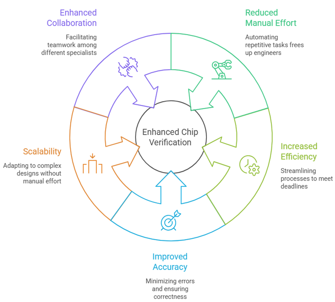
The integration of AI and formal verification techniques offers several advantages that can transform the chip verification landscape:
- Reduced Manual Effort: AI can significantly reduce the manual effort required by automating many aspects of the verification process. Engineers can focus on more complex tasks, such as analyzing results and refining designs, rather than spending time on repetitive verification tasks.
- Increased Efficiency: Combining AI and formal techniques streamlines the verification process, allowing teams to meet tight deadlines without compromising quality. This increased efficiency can lead to faster time-to-market, giving companies a competitive edge.
- Improved Accuracy: Both AI and formal techniques enhance the accuracy of verification processes. AI reduces human error in test generation and analysis, while formal methods provide a mathematical guarantee of correctness. This dual approach leads to higher confidence in the final product.
- Scalability: As designs become complex, traditional verification methods may need help to keep up. The scalability of AI and formal techniques allows verification processes to adapt to increasingly complex designs without increasing manual effort. This scalability is particularly important for modern multi-die systems, chiplet architectures, and high-performance SoCs.
- Enhanced Collaboration: AI tools often come with user-friendly interfaces that facilitate collaboration among team members. This can help bridge gaps between hardware engineers, software developers, and verification specialists, fostering a more cohesive development environment.
Partner With Tessolve To Elevate The Chip Design And Verification Process
In the fast-paced semiconductor industry, partnering with Tessolve can significantly enhance your integrated chip design and verification processes. Tessolve is renowned for its expertise in custom chip design, providing tailored solutions for analog, digital, and mixed-signal projects.
Leveraging advanced AI and formal verification techniques, Tessolve streamlines the verification process, reducing manual effort and accelerating time-to-market. By utilizing modern EDA methodologies and scalable verification frameworks suited for advanced semiconductor architectures, Tessolve helps organizations manage increasing design complexity efficiently.
Tessolve’s scalable solutions adapt to project complexity, allowing flexibility in responding to market demands. Our collaborative environment fosters close communication, ensuring that your strategic objectives are met.
By partnering with Tessolve, you gain access to industry-leading expertise and innovative verification methods, empowering you to navigate the challenges of semiconductor development effectively. Enhance your chip design processes and achieve superior product quality by choosing Tessolve as your trusted partner.
Let’s Sum Up
The landscape of integrated chip design is evolving rapidly, demanding innovative approaches to verification. By integrating AI and formal techniques, semiconductor companies can significantly reduce manual effort, enhance accuracy, and improve efficiency in the verification process. These advancements allow engineers to focus on more complex tasks and adapt to the growing complexity of designs.
As semiconductor architectures move toward advanced nodes, heterogeneous integration, and increasingly complex SoC designs, intelligent verification strategies become essential for maintaining reliability and performance.
Partnering with experts like Tessolve offers tailored solutions that streamline the custom chip design and development lifecycle, ensuring high performance and reliability. Embracing these modern verification strategies accelerates time-to-market and positions companies at the forefront of semiconductor innovation.
Frequently Asked Questions
- What are the leading trends in AI-based chip architecture and verification?
Leading trends include AI-driven architecture exploration, Agentic AI for EDA workflows, AI-assisted verification planning, ML-based coverage prediction, and intelligent debugging systems that accelerate validation for complex SoCs and chiplet-based designs.
- How does AI enhance verification and validation in IC design?
AI enhances IC verification by automating test generation, prioritizing failures, predicting coverage gaps, and accelerating debug cycles, allowing engineers to identify complex design bugs earlier and achieve faster verification closure.
- Why is chip verification critical in semiconductor design?
Chip verification ensures that a design functions correctly before fabrication. It helps detect design flaws, validate specifications, and prevent costly silicon re-spins during the semiconductor development process.
- How does AI improve chip verification workflows?
AI automates tasks like test generation, debugging, and coverage analysis. It also learns from past verification runs to optimize verification strategies and accelerate coverage closure.
- What is the role of formal verification in chip design?
Formal verification uses mathematical proofs to confirm design correctness. It helps identify deep logic bugs and corner cases that traditional simulation-based verification might miss.