Designing a single Printed Circuit Board (PCB) is challenging enough; now imagine designing several boards that all need to connect, communicate, and cooperate without frying each other. That’s multi-board system design in a nutshell.
It’s not just about stacking PCBs and linking them with connectors. It’s about synchronizing layouts, coordinating mechanical design, ensuring power integrity, and ensuring that when you press the “power on” button. The whole system behaves as one harmonious unit, not a confused collection of boards.
Let’s dive into how to keep multi-board designs sane, practical, and production-ready.
Why Engineers Go Multi-Board (and Why It’s Worth the Trouble)
Sure, a single board might sound simpler, but multi-board systems often make more sense, especially for complex electronics.
Common Reasons to Use Multi-Board Designs
- Modularity: You can reuse certain boards (like compute or power modules) across different products.
- Manufacturing Flexibility: Smaller boards are easier (and cheaper) to fabricate and test individually.
- Thermal Management: Heat-generating components can be placed on separate boards for better airflow.
- Noise Isolation: Keeping analog and digital sections apart reduces interference.
That said, more boards mean more complexity, especially in signal routing, synchronization, and mechanical integration.
Key Steps to Designing and Synchronizing Multi-Board Systems
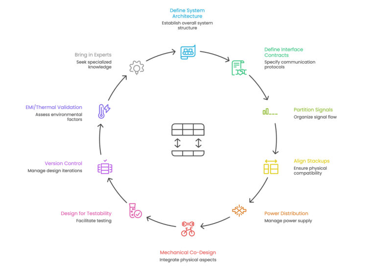
Step 1: Start with a System-Level Architecture
Before you drop a single trace, begin with a system-level block diagram. This visual map defines where every major function lives and how each board interacts with the rest.
What Your Diagram Should Include
- Each board’s role (e.g., power, logic, RF, I/O)
- Communication links (SPI, USB, Ethernet, etc.)
- Power paths and return routes
- Mechanical relationships (stacking, cabling, connectors)
This document serves not merely as a record but rather as your comprehensive guide to design principles. Update it every time something changes, and make sure everyone is literally “on the same page.”
Step 2: Define Clear Interface Contracts
When multiple teams (or even individuals) work on separate boards, interface discipline becomes vital.
Interface Contract Essentials
- Signal Classes: Define which lines carry what, such as digital, analog, or mixed-signal.
- Impedance & Timing: Specify impedance targets, trace lengths, and delay budgets.
- Power Delivery: Document voltage levels, sequencing, and load requirements.
- Mechanical Fit: Include tolerance margins for connectors, board spacing, and screw holes.
Changing a connector pinout mid-design without informing others? That’s how projects go from “on track” to “on fire.”
Step 3: Partition Signals Intelligently
Some signals should stay local; others need to hop between boards. Choose wisely.
Tips for Smarter Partitioning
- Keep high-speed buses (PCIe, DDR, LVDS) on the same board when possible.
- For inter-board high-speed connections, use differential pairs and controlled impedance connectors.
- Place serializers/deserializers (SerDes) near connectors to reduce trace length and crosstalk.
A well-thought-out PCB design board plan saves you from later scrambling to fix signal integrity issues that could’ve been avoided.
Step 4: Align Stackups Across Boards
One of the biggest headaches in multi-board systems is mismatched layer stacks. If your main logic board has an 8-layer stack with ground and power planes, but your secondary board has 4 layers and a different dielectric, guess what, your signal return paths might not line up.
Stackup Synchronization Checklist
- Use consistent impedance models.
- Ensure signal reference planes align at board interfaces.
- Simulate interconnect transitions (especially for high-speed lines).
- Coordinate with your PCB layout service provider early.
If different materials are used (like FR4 for logic and Rogers for RF), adjust trace geometry to keep impedance continuous.
Step 5: Power Distribution: Beyond Just Decoupling
Power delivery in multi-board systems isn’t just about slapping on capacitors. You have to model the PDN (Power Distribution Network) through every connector and cable.
Things to Remember
- Place bulk capacitors close to connectors.
- Simulate inrush current and voltage drops across connections.
- Add isolation and transient protection between boards.
Think of power like traffic; bottlenecks happen at junctions. Treat connectors as critical PDN components.
Power Distribution Network in PCB Design: Ensuring Stable Power Delivery
Step 6: Don’t Ignore Mechanical Co-Design
Electrical design is only half the job. Mechanical fit is where things can fall apart, literally.
Good Practices for Mechanical Co-Design
- Use 3D STEP models for every board and connector.
- Check enclosure clearances early using 3D mockups.
- Keep connector insertion and removal forces in mind.
- Validate all mounting points and standoffs.
- Validate component placements in all boards if they stay within the recommended height restrictions and keepout areas – Final validate shall be before gerber release
An otherwise perfect PCB design can still fail because a connector doesn’t align by 1 mm.
Step 7: Design for Testability
Once your boards are stacked, test access gets tough. Plan for it up front.
Multi-Board Testability Tips
- Add test headers and access pads before routing is finalized.
- Coordinate with test engineers on fixture compatibility.
- Design JTAG or boundary-scan chains that can span multiple boards.
A little forethought here saves a lot of pain during bring-up.
Step 8: Version Control and Cross-Team Coordination
If Board A changes a connector pin, Boards B and C must update immediately. Maintain a living document that tracks all inter-board dependencies.
How to Stay Organized
- Use shared repositories for schematics and layouts.
- Maintain an Interface Control Document (ICD).
- Set up release gates; no one releases until all dependent teams sign off.
It’s not bureaucracy; it’s survival.
Step 9: EMI, Thermal, and System-Level Validation
Multi-board assemblies are essentially one big EMI generator waiting to happen. And don’t even start on thermal.
Keep These in Mind
- Separate noisy switching regulators from sensitive analog circuits.
- Use shields strategically (not everywhere).
- Simulate airflow and heat transfer between boards.
- Do early pre-compliance scans at the system level.
Step 10: When to Bring in Experts
Sometimes, the best move is to get help. A specialized PCB design service or PCB layout service can accelerate your project timeline, validate your signal integrity, and optimize manufacturability.
They’ve seen it all, from multi-board RF systems to high-speed communication platforms — and they know what’s likely to fail before you do.
Tessolve: Powering the Next Generation of Electronic Systems
At Tessolve, we take multi-board complexity and make it manageable. Our hardware design experts offer full-spectrum engineering, from concept and schematic to simulation, layout, and validation. With our advanced PCB design service and PCB layout service, we help clients build high-performance systems that meet thermal, EMI, and manufacturability requirements right from the first prototype.
Our PCB design board engineers have extensive experience in HDI, high-speed digital, RF, and mixed-signal PCB design for industries like automotive, telecom, and semiconductors. Beyond layout, our teams handle mechanical co-design, test development, and system validation, making Tessolve a trusted one-stop solution for end-to-end hardware innovation.
If you’re building a complex multi-board system, Tessolve can bring the precision, collaboration, and speed your design truly deserves.
FAQs
What is multi-board system design in electronics?
It’s the process of creating multiple interconnected PCBs that work together as a single functional system.
Why is synchronization important in multi-board PCB design?
Proper synchronization ensures signal integrity, timing accuracy, and reliable power delivery across all interconnected boards.
How can I avoid errors in multi-board integration?
Maintain interface control documents, align stackups, and involve a professional PCB layout service early in development.
Why choose Tessolve for multi-board system projects?
Tessolve provides expert PCB design service, Signal and Power Integrity Simulation, Mechanical design and validation to ensure high-performance, manufacturable multi-board systems.