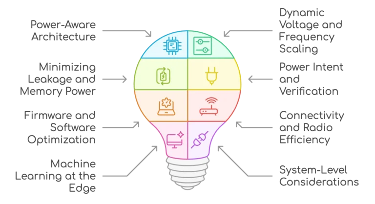
The demand for mobile and IoT devices is rapidly expanding, fueled by smart homes, wearables, industrial automation, and connected healthcare. At the core of these devices lies the system-on-chip (SoC), a compact powerhouse that integrates processing, memory, connectivity, and sensor interfaces into one silicon package.
The challenge? Balancing performance and feature-rich functionality with ultra-low power consumption. For mobile phones, long battery life is a selling point. For IoT devices, many of which run on coin cells or energy harvesting, power efficiency is the difference between success and obsolescence. This is where chip design strategies focused on energy efficiency come into play.
In this blog, we explore the critical approaches and technologies that enable low-power SoC development for mobile and IoT devices.
Why Low-Power SoC Design Matters Today
Low-power design has become a defining factor for next-generation electronics. Users expect longer battery life in smartphones, wearables, and wireless earbuds, while industries deploying IoT sensors require devices that can run unattended for years. At the same time, the complexity of SoCs is growing, with AI acceleration, advanced connectivity, and higher integration levels increasing power demands.
This creates a paradox: more features, but less energy budget. The solution lies in adopting advanced methods pioneered by chip design companies and supported by chip design software companies, ensuring energy efficiency without compromising user experience.
Critical Strategies and Technologies for Low-Power SoC Design

1. Power-Aware Architecture
Energy efficiency starts at the architecture level. Successful chip design companies begin with well-defined power budgets aligned with device use cases, whether it’s always-on sensing, bursty communication, or local AI processing.
Architectural strategies include:
- Always-On Domains: Creating tiny, low-leakage domains that manage wake-up events while the main system sleeps.
- Heterogeneous Processing: Using specialized cores (DSPs, NPUs, or low-power MCUs) for specific workloads to reduce overall energy per operation.
- Event-Driven Processing: Ensuring the chip wakes only for meaningful data, minimizing wasted cycles.
2. Dynamic Voltage and Frequency Scaling (DVFS)
DVFS remains one of the most effective methods of saving energy in SoCs. By adjusting clock speed and voltage according to workload intensity, devices can achieve optimal performance without burning unnecessary power.
Advanced implementations now leverage Adaptive Voltage and Frequency Scaling (AVFS), which dynamically tunes operating conditions based on process and temperature variations. This approach, often supported by advanced chip design software companies, ensures efficiency across multiple real-world scenarios.
3. Minimizing Leakage and Memory Power
Leakage current is a growing challenge at advanced process nodes. Techniques like using high-threshold voltage (high-Vt) cells, multi-Vt libraries, and power gating help suppress leakage in idle modes.
Equally important is memory optimization. Since memory accesses consume significant energy, designers adopt strategies such as scratchpad memories, compression, and near-memory computing. By minimizing off-chip memory traffic, SoCs reduce one of their largest power drains.
4. Power Intent and Verification
Modern chip design requires power intent to be captured from the very beginning using Unified Power Format (UPF) or Common Power Format (CPF). This ensures that power domains, retention strategies, and isolation logic are implemented consistently across design and verification.
Power-aware verification further ensures that low-power techniques like clock gating, domain switching, and state retention work seamlessly in real silicon. Chip design companies that invest heavily in these methodologies reduce the risk of late-stage power failures.
5. Firmware and Software Optimization
Even the best hardware can fall short if the software isn’t optimized for low power. Firmware strategies include:
- Tickless RTOS modes for longer sleep times.
- Peripheral-driven DMA to reduce CPU activity.
- Power-aware APIs that let applications signal latency requirements.
This co-design of hardware and software ensures that low-power features are not only built into the SoC but also leveraged effectively by the system.
6. Connectivity and Radio Efficiency
Wireless communication often consumes more power than computation in IoT devices. Optimizing radio duty cycles, selecting energy-efficient communication standards (e.g., BLE, NB-IoT), and leveraging hardware-based encryption help extend battery life significantly.
By integrating efficient radio subsystems, SoCs can balance connectivity needs with power efficiency, a critical consideration in IoT environments.
7. Machine Learning at the Edge
As IoT devices increasingly adopt AI features, energy-efficient machine learning is crucial. TinyML techniques, such as model quantization, pruning, and hardware acceleration, allow inference at low power budgets.
Specialized NPUs and DSPs enable local execution of tasks such as keyword spotting or anomaly detection, eliminating the need to send data to the cloud while consuming only milliwatts. Chip design software companies play a key role here by providing optimized toolchains for low-power AI deployment.
8. System-Level Considerations
Low-power SoC design cannot exist in isolation. It must be co-optimized with:
- Power Management ICs (PMICs): Ensuring fast and efficient voltage scaling.
- Battery Systems: Matching discharge profiles with SoC power modes.
- Thermal Design: Preventing hot spots that increase leakage.
- Packaging: Reducing parasitics in 2.5D or 3D integration.
These system-level elements are critical for sustaining low-power operation in real-world devices.
10 Ways Low Power VLSI Design Enables Smarter and Greener Tomorrow
Tessolve: Driving Innovation in Low-Power SoCs
At Tessolve, we specialize in enabling semiconductor innovation with a strong focus on low-power SoC development. Our end-to-end engineering services cover architecture, design, verification, DFT, and physical implementation, along with post-silicon validation and embedded systems. With deep expertise in UPF-based power intent, clock and power gating, DVFS enablement, and memory optimization, we help customers achieve unmatched energy efficiency in their SoCs.
Our global labs are equipped for advanced test engineering, system-level validation, and low-power characterization, ensuring that power savings translate from simulation to real silicon. Backed by decades of experience and a worldwide presence, we provide the scalability and technical depth needed for today’s mobile and IoT innovations. Contact us now to explore how Tessolve can accelerate your next low-power SoC.


