
In the evolving world of chip design, RTL design for AI workloads has emerged as a critical frontier. As artificial intelligence systems continue to demand more compute capacity, energy efficiency, and effective data movement at the RTL (Register‑Transfer Level) have become essential design targets. AI workloads pose unique challenges in terms of parallelism, memory access patterns, and power constraints. These challenges are pushing teams across chip houses and even the top semiconductor companies to innovate in hardware architectures and RTL strategies.
The RTL Challenge Under AI Workloads
RTL designers must craft dataflow pipelines that can feed matrix multiply engines, neural processing arrays, or tensor cores at massive scales. Traditional RTL design techniques that optimize for clock frequency or area need to be extended to effectively manage data locality, buffering strategies, and voltage/frequency scaling. In AI SoCs, a careful balance between low-power states and sustained performance bursts is essential.
Designers working in a semiconductor engineering environment must build RTL architectures that allow data movement close to computation (e.g., scratchpad memories, systolic arrays), reducing long-distance transfers that cost energy and latency. Efficient use of bus architectures, hierarchical memory banks, and power gating also becomes vital.
Power Efficiency via RTL Techniques
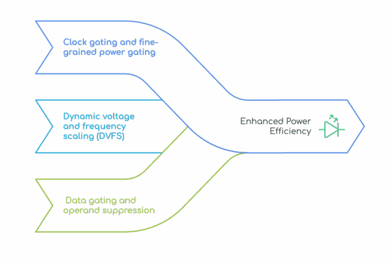
Power efficiency isn’t new in RTL design, but AI workloads amplify its importance:
- Clock gating and fine-grained power gating: RTL modules idle unless active, preserving energy in large AI accelerators.
- Dynamic voltage and frequency scaling (DVFS): RTL must support multiple P‑states, enabling AI engines to down‑throttle during lower workload phases.
- Data gating and operand suppression: Idle data lanes or negligible-value macros can be disabled to avoid wasted switching.
These techniques are widely adopted across semiconductor design company teams and labs aiming at top-tier chip products.
Efficient RTL Design Strategies for VLSI Integration
Data Movement: Locality, Bandwidth, and Memory Partitioning
AI workloads typically involve dense, multi‑dimensional matrix ops that stress memory systems. RTL architects carefully partition memory banks to match access patterns:
- Systolic array mapping: Breaking down large tensor operations into tiled compute blocks that stream data in a controlled, local fashion.
- Double‑buffering and ping‑pong FIFOs: Allowing compute units to process one tile while fetching the next, without stalls.
- Hierarchical scratchpad and cache: Near‑compute SRAM blocks reduce traffic to global caches or off-chip DRAM, saving both power and latency.
In the context of a top semiconductor company, these techniques are part of rigorous RTL design for AI accelerators. A successful semiconductor design company will incorporate automated RTL generation flows, aided by AI in some cases, to explore design trade‑offs efficiently.
Role of Automation and AI in RTL Design Flows
Modern design flows increasingly utilize AI and automation during RTL development:
- High‑level synthesis (HLS) with AI‑guided exploration can generate RTL that meets power/performance targets efficiently.
- Internal AI tools can predict hotspots, power leakage paths, or data congestion via simulations across RTL test vectors.
- Verification workflows can be AI‑driven, e.g., auto-generation of assertions, constraint optimizations, or intelligent testbench generation, to speed up RTL validation.
These capabilities are increasingly standard in semiconductor engineering teams working on AI SoCs.
Power-Performance-Area (PPA) Trade‑offs and RTL Tuning
Designing RTL for AI workloads means balancing PPA trade‑offs:
- Area: Larger register files or more memory banks reduce data movement cost, but increase die size.
- Performance: High throughput demands high clock rates or parallel pipelines, but these increase power unless balanced with gating.
- Power: Minimizing switching, leakage, and memory access energy is key, especially for edge or mobile AI devices.
Tools built by a semiconductor design company help explore these trade‑offs via RTL parameter sweeps, simulations, and floorplanning guidelines.
How to Achieve Better PPA (Power, Performance, Area) in VLSI Design
Case study: AI Accelerator RTL Integration
Consider a neural network accelerator integrated into an SoC. The RTL design flow might include:
- Topology mapping: Systolic array dimensions chosen to fit workload sizes.
- Memory partitioning: Scratchpads sized for tiled computation; FIFO depth tuned to avoid stalls.
- Power domains: Activation units, accumulation banks, and control logic are placed in separate domains for gating.
- Turn off unused lanes: Clock and power gating logic added during RTL synthesis to turn off unused lanes.
- DVFS support: RTL registers and interface logic include hooks for dynamic scaling.
- Data gating: Null or zeros masked to avoid toggling.
- Automation tools: AI-guided synthesis to reduce congestion or timing slack.
Such an RTL pipeline requires collaboration between chip designers, verification teams, floorplan engineers, and system architects. This collaboration often takes place within advanced semiconductor engineering environments found at a top semiconductor company.
Verification and Data Movement Correctness
Data movement correctness is essential. RTL must ensure:
- No buffer overflows or underflows in stream interfaces.
- Bandwidth constraints (e.g., DRAM throughput) aren’t violated.
- Timing closure across multiple domains is sound.
AI‑assisted verification, part of an advanced semiconductor design company offering, can significantly reduce verification cycle time while improving coverage.
Future Trends in RTL Design for AI Workloads
Looking ahead, RTL flows will evolve with these trends:
- Chiplets and modular design: Partitioning accelerator blocks into reusable RTL modules with coherent data interfacing.
- Neuromorphic and in‑memory compute: RTL for non‑Von Neumann AI engines, requiring novel power/data movement strategies.
- AI‑driven RTL synthesis and verification: More widespread use of AI guidance in design exploration, assertion generation, and functional coverage.
These advances are likely to be spearheaded by teams in semiconductor engineering, including those at the top semiconductor companies.
Why Focusing on Power and Data Movement Matters
In summary, designing RTL for AI workloads demands a holistic view of power efficiency and data movement. Without efficient gating, buffering, and on‑chip routing, AI engines waste energy and incur latency. Effective design demands:
- RTL architectures that localize data closely.
- Fine‑grained control over gating and DVFS.
- Automation and AI tools for rapid exploration and verification.
These capabilities define the difference between average implementations and those delivered by a premier semiconductor design company engaged in advanced semiconductor engineering.
Tessolve: Your Partner in AI‑Optimized RTL Design
At Tessolve, we specialize in delivering RTL designs that meet the unique demands of AI workloads. As a top semiconductor company with deep expertise in semiconductor engineering, we help our clients optimize for power efficiency and data movement from architecture to post‑silicon.
Here’s how we make a difference:
- End‑to‑End RTL Expertise: From initial specification to RTL coding, synthesis, and verification, our teams ensure designs meet stringent AI workload requirements.
- Power & Data Movement Optimization: We integrate advanced gating techniques, localized memory architectures, and efficient interconnect strategies to reduce energy use and latency.
- AI‑Assisted Design & Verification: Leveraging automation and AI tools, we accelerate design exploration, improve verification coverage, and reduce time‑to‑market.
As a trusted semiconductor design company, Tessolve combines technical excellence with robust infrastructure to deliver high‑performance, power‑efficient AI silicon solutions that keep you ahead in a competitive market.