
The relentless pursuit of miniaturization in the semiconductor industry has led to remarkable advancements over the decades. However, as traditional scaling approaches encounter physical and economic limitations, the industry has been compelled to explore alternative solutions. In this situation, there has been a great deal of thinking about 3D-ICs as a new high-density integration technology to carry forward the momentum of VLSI design. The present article discusses a brief overview of 3D-ICs, their significance in elevating VLSI design, and the happenings in the area of chip design companies.
The Evolution of Integrated Circuits and the Emergence of 3D-ICs
Integrated Circuits (ICs) have been, and still are, the great enablers of modern electronics, allowing for the integration of millions and billions of transistors onto a single chip. In simple terms, this development, popularly characterized by Moore’s Law, has led to phenomenal growth in computing capability through almost exponential increases. However, now that transistors are reaching atomic dimensions, high power density problems, heat removal, and short-channel effects have become prevalent in the past decade or so.
In order to overcome these challenges, the industry has looked into alternate integration techniques; amongst which, 3D-ICs have now emerged as a possible candidate for consideration. Instead of working in a traditional two-dimensional layout, 3D-IC stacks multiple layers of active electronic components on top of one another and interconnects such layers using techniques like Through-Silicon Vias (TSVs).
- There are a number of perceived benefits associated with the said architecture, including:
- Enhanced Performance: 3D-ICs can achieve faster signal transmission and lower latency by reducing the distance between interconnected components.
- Improved Power Efficiency: Shorter interconnects result in reduced power consumption, addressing one of the critical concerns in modern VLSI design.
- Increased Functional Density: Vertical stacking allows for more functionality within a given footprint, enabling the integration of heterogeneous components such as processors, memory, and sensors on a single chip.
Implications for VLSI Design

The advent of 3D-ICs has profound implications for Very-Large-Scale Integration (VLSI) design methodologies:
- Design Complexity: Designing 3D-ICs introduces new challenges in thermal management, signal integrity, and power distribution. VLSI design companies must develop advanced tools and methodologies to address these complexities.
- EDA Tool Evolution: Electronic Design Automation (EDA) tools need to evolve to support 3D design paradigms. Leaders in the EDA industry, such as Synopsys and Cadence Design Systems, are at the forefront of developing solutions that cater to the unique requirements of 3D-ICs.
- Testing and Verification: The stacked nature of 3D-ICs necessitates novel testing strategies to ensure reliability and performance. This has led to the development of specialized testing protocols and equipment.
The Role of Chip Design Companies in the 3D-IC Era
As the semiconductor landscape shifts towards 3D integration, chip design companies are adapting to harness the potential of this technology:
- Strategic Collaborations: Companies are forming alliances to pool expertise and resources. For instance, MIPS has shifted its strategy towards designing chips for AI-enabled robots, focusing on sensing, action calculation, and motor control. This move aligns with the industry’s trend towards specialization and collaboration to tackle the complexities of modern chip design.
- Investment in R&D: Significant investments in research and development are being made to overcome the technical challenges associated with 3D-ICs. For example, Synopsys has projected its second-quarter revenue to surpass Wall Street expectations due to heightened demand for its chip design software, mainly driven by the surge in AI chip development.
- Government Partnerships: Governments are recognizing the strategic importance of semiconductor technology. Malaysia, for instance, will pay Arm Holdings $250 million over the next ten years for high-end chip design blueprints to support its ambitions of producing its own graphics processing unit chips within five to ten years.
Challenges and Considerations in 3D-IC Adoption
While 3D-ICs offer numerous benefits, their adoption is accompanied by several challenges:
- Thermal Management: Stacking active components increases power density, necessitating advanced cooling solutions to prevent overheating.
- Manufacturing Yield: The complexity of 3D stacking can impact manufacturing yields, affecting the overall cost-effectiveness of the technology.
- Standardization: The industry lacks standardized design and manufacturing processes for 3D-ICs, leading to potential interoperability issues.
3D ICs, Chiplets & HBM: How Packaging Is Driving the Semiconductor Roadmap
The transition to 3D-ICs signifies a paradigm shift in the semiconductor industry. As VLSI design companies and chip design companies continue to innovate, we can anticipate:
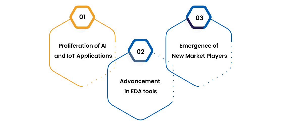
- Proliferation of AI and IoT Applications: Further advancement in performance and integration of 3D-IC will promote the high level of development of AI and IoT, a boost toward smarter and connected environments.
- Advancement in EDA tools: The EDA tool-providing companies shall keep evolving and moving ahead with incorporation of AI-based design and verification tools to manage the complexity that has arisen with the introduction of 3D-IC.
- Emergence of New Market Players: The continuous evolution may create new opportunities for designers of chips, firms that still specialize in 3D integration, offering competition and innovation.
Let’s Conclude
3D-ICs constitute a critical revolution aimed at higher-density integration in semiconductor technologies. The vertical stacking of components offers remedial solutions to the limitations of traditional scaling mechanisms. As this technology gains traction in industry, VLSI design companies as well as chip design firms must find ways to respond to the challenges it brings through innovation, collaboration, and strategic investment. Undoubtedly, the successful embrace of 3D-ICs will bring about the next generation of electronic devices with unmatched performance and functions.
Tessolve: Pioneering 3D-IC Integration in VLSI Design
In the domain of semiconductor innovation, Tessolve offers end-to-end solutions that practically dovetail with the latest improvements in the 3D-IC technology arena. Our lineup includes everything from IC package design, chip design, and post-silicon services, which are intrinsic to 3D-IC realization. We offer connective and seamless solutions right from design conceptualization to tape-out. Tessolve also ensures optimized, scalable and highly reliable silicon solutions. Therefore, Tessolve would be an ideal partner for an organization that aims to harness the potential of 3D-IC in the design of our VLSI project.


