With the semiconductor advancement, the digital world is demanding more and more electronic products from engineers. This makes the engineering job more complex and bigger in scope. That’s where AI has revolutionized the chip industry by playing a pivotal role in modern-day chip design.
Electronic Design Automation (EDA) tools are software applications that VLSI chip design engineers utilize during the design and development of electronic systems, including chip design. AI in EDA tools enhances and automates the various stages of the design process by leveraging AI methodologies, such as machine learning and deep learning. These tools can analyze large datasets, recognize patterns, and make data-driven decisions. This aids engineers in exploring design spaces more effectively and addresses the growing complexity of modern electronic systems. This blog will delve deeper into the need for AI in chip design, its benefits, and applications.
Decoding the Design Engine: A Look at AI-Powered EDA Tools
EDA is a set of software, hardware, and essential services used for chip design and semiconductor development. Due to billions of connections and multi-team collaborations, EDA software plays a vital role in chip production by ensuring precise simulation, efficient design, and effective verification.
This simulated environment allows chips to be analyzed and optimized for performance before entering real-world production. Over time, AI in EDA tools has transformed this process, integrating intelligence into everything from circuit simulation to layout optimization, thus reducing the time-to-market and improving chip quality.
What Makes AI Crucial for Chip Design?
The complexity of chip design is increasing daily due to advancements in semiconductor technology, such as advanced process nodes, quantum dots, heterogeneous integration, etc. This has led to unprecedented challenges for VLSI hardware design engineers. That’s where AI has emerged as a powerful solution, aiding in silicon quality and productivity in designing smaller PCB designs.
Engineers face numerous possibilities while designing, verifying, and testing the chip for new-age electronics design. So, they find the best-case scenario for better power, performance, and area, as they need to bind numerous transistors into one design. Incorporating AI has increased chip design productivity, quality, and efficiency, and reduced design costs.
Key Advantages of Using AI-Powered EDA Tools for Chip Design
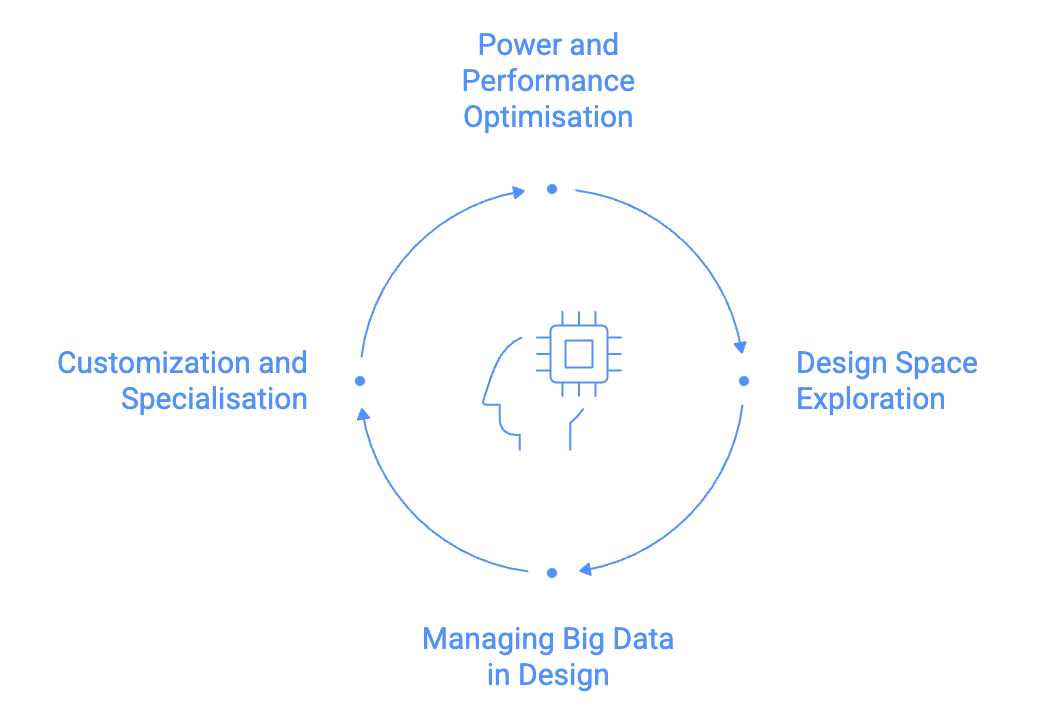
Power and Performance Optimisation
AI aids in simultaneously optimizing chip designs for power consumption and performance, a critical factor in today’s electronics. Machine learning algorithms, particularly Reinforcement Learning (RL) agents, can assess and forecast how various design decisions (e.g., transistor sizing, wire routing) will affect Dynamic Power and Leakage Power, resulting in more energy-efficient and high-frequency solutions.
Design Space Exploration
AI makes it possible to investigate the design space in greater detail than manual or traditional search algorithms. AI-driven technologies (e.g., Synopsys DSO.ai) can find the best trade-offs and solutions by simultaneously considering many design aspects and settings across the entire PPA envelope. These are complex, multi-variable trade-offs that are computationally prohibitive for human designers to examine manually.
Managing Big Data in Design
A large amount of data, including simulation logs, verification coverage, and manufacturing yield data, is produced during the simulation, verification, and testing phases of the semiconductor design process. AI technologies may analyze terabytes of datasets quickly to derive actionable insights, predict design failures, and make data-driven decisions that enhance design quality and yield predictability.
Customization and Specialisation
AI allows for the development of specialized, high-performance chips tailored for specific applications. EDA tools for AI chip design are particularly useful for creating accelerators optimized for AI workloads, enhancing computational speed, and reducing energy use in AI-driven applications.
Power-Efficient Chip Design for the IoT Era
How AI EDA Integrates with Traditional EDA Flows
AI-powered EDA tools are not replacing the established design flow (RTL to GDSII); instead, they are integrating at key choke points to act as intelligent optimizers or “co-pilots.” This integration primarily occurs in two ways:
1. AI Inside the Tool (Internal Solver Enhancement)
- Function: AI models are integrated directly into existing EDA algorithms (e.g., those for placement, routing, or timing analysis).
- Mechanism: Machine Learning models are trained on large historical datasets of successful designs and simulation runs to replace or enhance traditional heuristics and static algorithms.
- Benefit: This leads to solver-level performance gains (e.g., faster runtime, higher-quality results in one step) because the AI has deep access to the internal data structures and physics-based solvers.
2. AI Outside the Tool (Autonomous Optimization Loop)
- Function: An AI engine (often an RL agent or Bayesian optimizer) acts as a smart design manager that sits on top of the entire EDA flow.
- Mechanism: The AI agent launches multiple runs of traditional EDA tools (e.g., synthesis, place-and-route), analyzes the output PPA metrics, and then intelligently modifies the design constraints or tool parameters for the next iteration.
- Benefit: This enables autonomous design space exploration, allowing the system to converge on optimal PPA solutions much faster than a human engineer manually iterating the flow. It effectively automates the “human in the loop” optimization process.
Applications of AI in Chip Design

Design Space Exploration
AI-powered EDA tools revolutionize design by optimizing performance, power, and area (PPA). This analyzes data and identifies patterns, helping to achieve a balance and meet specifications. These tools excel in navigating the multifaceted design space, aiding informed decisions on power, performance, and area trade-offs. This proves invaluable in achieving VLSI physical design goals amid competing constraints. AI-powered EDA tools leverage machine learning to identify optimal design configurations, accelerating exploration and allowing designers to focus on efficient solutions.
Physical Design Automation
AI-powered EDA tools automate the physical design by optimizing the components’ arrangement. This enhances signal integrity, minimizes power consumption, and manages thermal considerations. Its predictive analysis is crucial in achieving timing closure by proactively addressing issues early in the design phase. This reduces the likelihood of last-minute adjustments.
Timing Closure and Verification
AI-powered EDA tools encompass predictive analysis, which extends to critical timing closure tasks. It forecasts potential timing issues, proposing preemptive solutions to streamline the process, reducing traditional time and effort.
AI’s role in VLSI board design verification utilizes machine learning techniques to enhance the process’s robustness. This recognizes complex patterns and potential design errors, making verification more efficient. This minimizes the risk of overlooking critical issues. In debugging and error correction phases, AI-powered EDA tools play a crucial role by automating the identification and correction of errors. This minimizes manual efforts, ensuring an efficient and reliable design verification process.
RTL to GDSII Flow
AI-powered EDA tools automate synthesis in the RTL to GDSII flow, swiftly generating optimized RTL designs for high-level specifications. This accelerates the design process, ensuring finely tuned RTL designs. For manufacturability, AI optimizes designs by considering lithography constraints, metal density, and yield, ensuring semiconductor devices meet design goals and are manufacturable at scale.
What’s Next in AI EDA
The application of AI in EDA is rapidly expanding into emerging and highly complex design domains:
- AI for Chiplet and 3D-IC Design: AI is essential for managing the skyrocketing complexity of chiplet architectures (2.5D/3D ICs). It optimizes partitioning, floorplanning, and crucial elements like signal integrity across high-bandwidth interfaces (e.g., UCIe), and manages the extreme thermal density of vertically stacked dies.
- AI for Analog/Mixed-Signal (AMS) Design: AI is automating traditionally manual AMS tasks. It uses RL agents to size transistors across numerous performance (PVT) corners intelligently and leverages ML for layout synthesis, guiding the placement and routing of sensitive analog components to minimize parasitic effects.
- AI for Quantum and Photonic EDA: For next-generation computing, AI is deployed to:
- Optimize Quantum Circuits: Aiding in the design and tuning of complex qubit layouts to minimize decoherence.
- Design Photonic Integrated Circuits (PICs): Optimizing the geometry and layout of optical components (e.g., waveguides, modulators) to reduce loss and enable robust electro-photonic co-simulation for high-speed AI accelerators.
The Role of EDA Software in Modern Chip Production
The EDA software role in chip production is expanding rapidly with AI integration. Traditional design workflows are being enhanced with machine learning-based automation for faster turnaround and reduced errors. EDA software helps semiconductor manufacturers simulate real-world chip behavior before fabrication, ensuring minimal redesign and cost savings.
With AI in EDA tools, chip developers can achieve unprecedented precision in power optimization, layout generation, and test automation. Whether designing AI chips or next-gen processors, AI-enhanced EDA solutions are redefining how chips are conceptualized, verified, and produced.
The Bottom Line!
AI-powered EDA tools are revolutionizing the chip design industry by automating various tasks and optimizing designs for better performance, power efficiency, and area. This not only reduces design costs and time to market but also allows engineers to explore a much larger design space than ever before.
Tessolve is a leading provider of engineering services and IT solutions for the global semiconductor industry. They offer a comprehensive suite of EDA services, including design for manufacturing (DFM) analysis, physical design, and verification. Tessolve can leverage its expertise in these areas to help chip designers adopt and integrate AI-powered EDA tools into their design flows, ensuring a smooth transition and maximizing the benefits of this transformative technology.
FAQs
1. How are leading EDA tools using AI to accelerate design verification?
Leading EDA tools use AI-driven analytics to automate verification, detect design issues, and accelerate debugging accuracy.
2. How does EDA software enable faster, more accurate chip production?
EDA software optimizes chip design, simulates real-world performance, and minimizes errors before manufacturing begins.
3. How does the EDA market support AI chip design and development?
The EDA market integrates AI algorithms to streamline design automation, enhance performance, and reduce production cycles.
4. Will AI completely automate chip design in the future?
Not entirely, AI complements engineers by automating complex tasks while improving creativity and design precision.


