Let’s Ensure The Design Resilience Of Designed ICs
Optimized Test Programs
With a talented pool of testing experts on the go
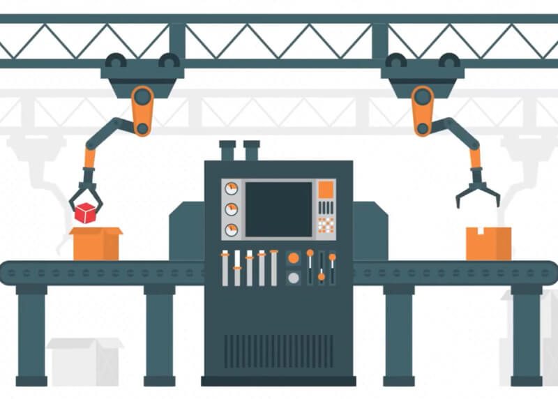
Validating output at each stage, from engineering to the final productization, is crucial as engineers push the limits of semiconductor and systems design. Semiconductor testing and validation practices must keep pace with the innovations and new design parameters and expectations being introduced. Our experts are competent in developing test solutions and simulation programs from scratch, supported with both probing and final testing of the design. Domain expertise is only one part of Tessolve’s differentiators. Robust testing infrastructure – testing labs across multiple locations, the latest test beds, and device characterization puts us ahead of the curve in semiconductor test engineering.
Spotlight On Competence
Infrastructure, SMEs, optimized processes

Test Solution for seamless transition from development to production and beyond.

Test Time Reduction, Yield Optimization, Platform conversions for new product designs as well as optimization of existing products.

First-in-class setup for test development – whatever the device, whatever the complexity, whatever the platform.

Focus areas include : Hi-end computing | Automotive | Power | 5G & RF | IOT (WLAN & Bluetooth) | Silicon Photonics
More On Test Engineering
Snapshot of our test-infra setup
1100+
+
Expert team of Test and Product engineers
900
+
Test programs released
30
+
And more ATE platform expertise and Custom solutions
30
%
Up to 30% Decrease in project cycle time

Furthering Our Testing Capability
A multitude of devices and practical testing know-how
Being in the semiconductor industry for almost two decades has enabled us to work on a varied type of test engineering solutions and services. From simple to complex to customized hardware and applications, we have been exposed to a multitude of devices. This has allowed us to develop deep knowledge as well as hands-on and diverse practical testing experiences.
Digital
Speed & Pin count, High Speed FPGAs & SoC FPGAs, High Performance 32 Bit Digital Signal Processors, Microprocessors, Microcontrollers, High speed Logic Ics & ASICs. We also provide compliance and margin analysis for the latest HSIO protocols, including PCIe Gen 6/7, DDR5/LPDDR5X/6, and CXL (Compute Express Link).
Analog Power & Automotive ASICs
Analog – Front End (AFE) Modules, High Speed Opamps, Precision Differential Amplifiers, Switches-Analog/Audio/Video/MIPI
Mixed Signal
ADC – 16 Bit, 24 Bit & DAC, Power Architecture® Processors, PLL , Multi-Channel 24-Bit Sigma Delta ADCs
RF/mm-Wav
5G/BT/WLAN/RADAR/Mobile Transceivers, Beam Formers, RF/mm_Wave Antenna Switches, Integrated Low Noise Amplifiers & Power Amplifiers
Sensors
Ultra High-Speed Line Scan Image Sensors, Area Scan Image Sensors, MEMS – Motion Sensor, Lidar and Radar Systems, and Automotive Grade Sensors.

Guarding the Gate: Advanced Silicon Security Testing
As products become increasingly connected, security is paramount. Our test programs incorporate advanced security validation techniques, including Fault Injection Testing, Side-Channel Analysis (SCA) Measurement, and comprehensive verification of Hardware Security Modules (HSMs) functionality to ensure silicon-level resilience against physical and cyber threats.
A Dedicated Infrastructure
State-of-the-art labs and custom test cells
Within our robust and established semiconductor testing infrastructure, our custom-built test cell is the pinnacle of specialized testing services, highly customizable to meet specific requirements. Our varied setups, ranging from CMOS Image Sensors to Rack & Stack setups, help in the process of providing quality and effective testing services. By developing a customized test cell, we are able to decrease test cost while maintaining test capability. We do this through building capability to either a rack and stack solution or a low-cost tester.
Tessolve Labs At A Glance
Specialized testing services and test floor


Download Brochure
Test Engineering Capabilities
Our solutions allow a seamless transition from development to production and beyond. Explore our Test Engineering Expertise in detail.


