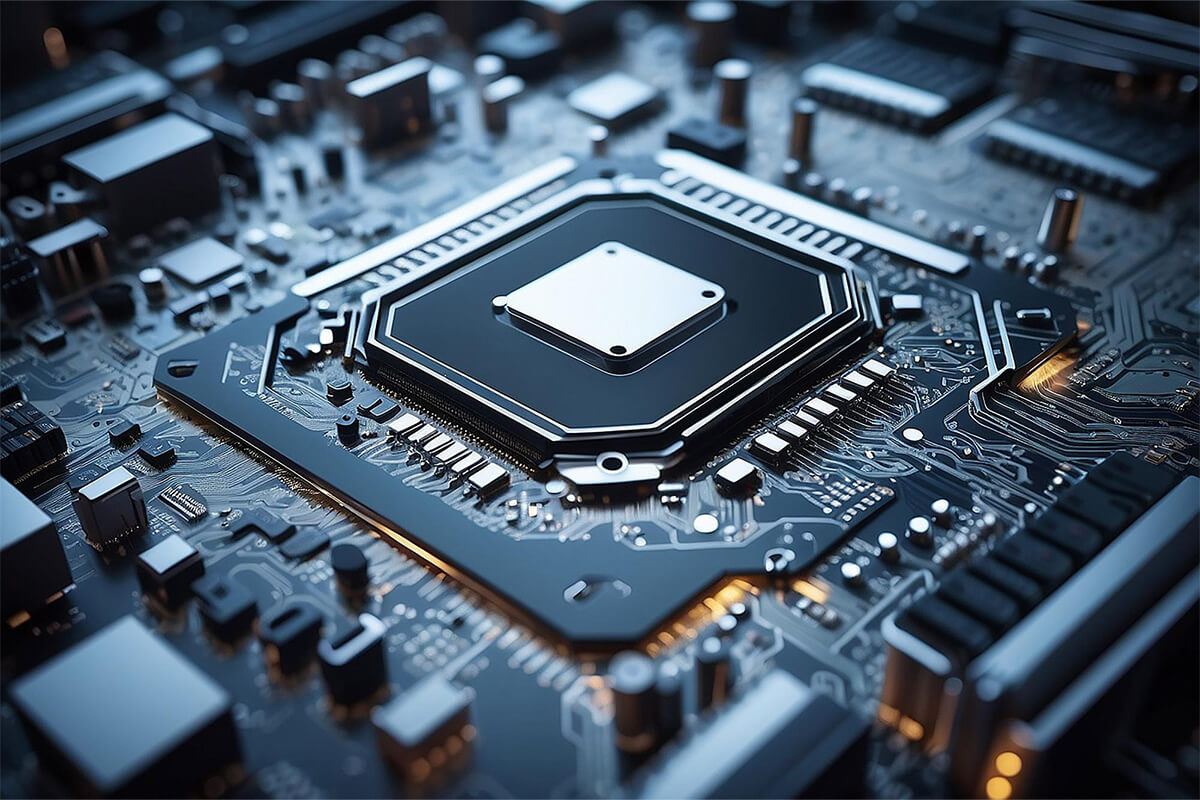
As VLSI chips continue to pack more and more transistors onto a single die, memory management becomes increasingly critical. The efficient utilization of on-chip memory resources directly impacts the performance, power consumption, and cost of these complex systems.
Employing innovative and efficient approaches to memory management is essential to unlock the full potential of a chip’s performance. Indeed, effective memory management is the cornerstone of successful VLSI design, laying the groundwork for optimal chip functionality and efficiency. Here are various design strategies and innovative approaches:
Memory Hierarchy Design:
Wireless testing is a critical process that ensures the functionality, security, and performance of wireless communication systems and devices. With the increasing reliance on wireless technologies, the need for robust testing strategies has become more significant than ever.
Memory hierarchy is a fundamental principle in VLSI chip memory management. This organizes memory subsystems in a hierarchical structure with varying speed, capacity, and cost characteristics. Registers and cache memory are at the top of the hierarchy, offering fast but limited storage for frequently accessed data. Main memory (DRAM) provides higher capacity but slower access times, while secondary storage devices like HDDs and SSDs offer more extensive storage but slower access.
Innovative approaches to memory hierarchy design aim to optimize memory organization and utilization. Cache partitioning divides cache memory into multiple partitions to accommodate different processing units or applications. Advanced prefetching algorithms and memory access scheduling techniques minimize memory access latency, enhancing system performance.
Non-Volatile Memory (NVM) Integration:
Non-volatile memory (NVM) technologies like RRAM, PCM, and MRAM offer persistent storage without constant power, suitable for applications needing persistent storage or fast boot times. Integrating NVM in VLSI hardware design optimizes memory management, leveraging unique characteristics for specific tasks. PCM’s fast read/write speeds make it ideal for cache memory in high-performance systems, while RRAM’s low power consumption suits energy-efficient embedded systems.
3D Memory Integration:
3D memory integration stacks memory components vertically, increasing memory density and interconnectivity. This addresses the demand for higher capacity and performance. Through-silicon vias (TSVs) enable vertical interconnects, while advanced bonding and stacking techniques ensure reliable integration.
Memory Compression and Decompression:
Memory compression reduces memory footprint by encoding data compactly, while decompression decodes it when accessed. These techniques lower memory bandwidth requirements and energy consumption, which benefits power-constrained environments like mobile and IoT devices. Reduced memory footprint allows more resources for critical functions, enhancing system efficiency.
Machine Learning-Based Memory Management:
Machine learning (ML) algorithms analyze system behavior and predict memory access patterns, dynamically adjusting memory allocation and scheduling. Trained on real-world memory access traces, ML models optimize memory management, improving performance and efficiency.
VLSI Circuit Basics: Understanding the Fundamentals
VLSI circuit creates integrated circuits (ICs) by combining thousands, millions, or even billions of transistors onto a single chip. VLSI circuit design involves the layout and interconnection of these ICs on a printed circuit board (PCB).
Decoding the Concept of VLSI Technology
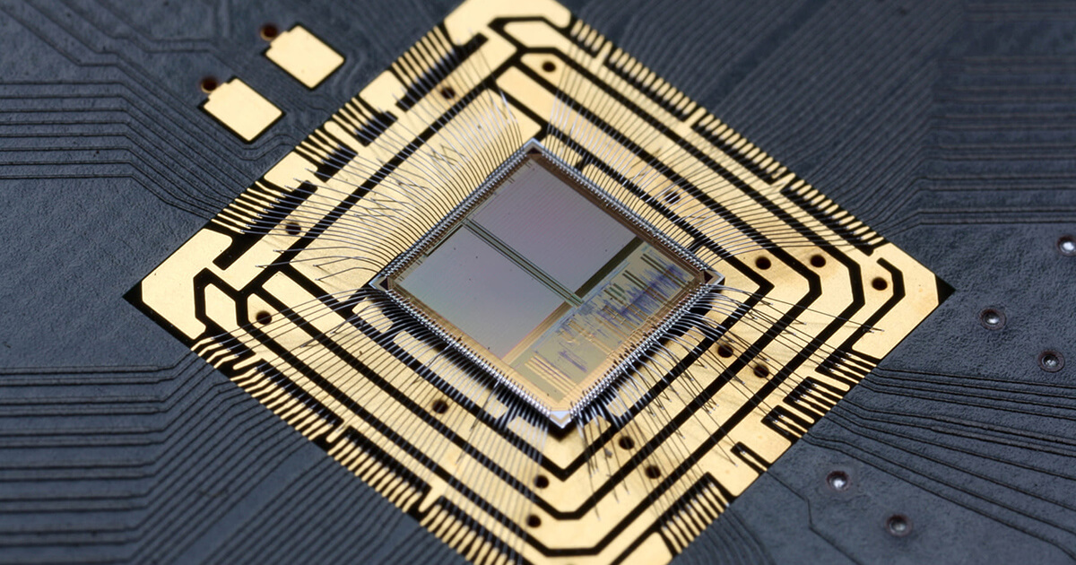
Integration Levels: VLSI refers to integrating many transistors onto a single chip. This integration can range from thousands to billions of transistors on a single IC.
Fabrication Processes: VLSI chips are typically fabricated using semiconductor manufacturing processes such as CMOS (Complementary Metal-Oxide-Semiconductor) technology.
Design Hierarchy: VLSI design follows a hierarchical approach, where complex systems are broken down into smaller functional blocks for more straightforward design and verification.
Design Flow
Specification: Define the requirements and specifications of the VLSI hardware design, including functionality, performance, power consumption, and size constraints.
Architectural Design: Develop the high-level architecture of the system, defining the major functional blocks and their interconnections.
RTL Design: Create the Register Transfer Level (RTL) description of the system using a Hardware Description Language (HDL) like Verilog or VHDL.
Synthesis: Convert the RTL description into a gate-level netlist using synthesis tools, which map the design to a library of standard cells.
Floorplanning and Placement: Determine the physical placement of the synthesized cells on the chip to optimize performance, power, and area.
Routing: Connect the placed cells with metal traces to establish interconnections while adhering to design rules and constraints.
Physical Verification: Perform design rule checks (DRC), and layout versus schematic (LVS) checks to ensure the design meets manufacturing requirements and matches the intended functionality.
Simulation and Verification: Use simulation tools to verify the functionality and performance of the VLSI design under different conditions and scenarios.
Manufacturing: Fabricate the VLSI chips using semiconductor manufacturing processes, such as photolithography, etching, and doping.
PCB Design Considerations
Component Selection: Choose appropriate ICs, passive components, and connectors based on the system requirements and performance criteria.
Signal Integrity: Ensure that signals transmitted between ICs and components maintain integrity to prevent data corruption and signal degradation.
Power Distribution: Design a robust power distribution network (PDN) to supply clean and stable power to all components on the PCB.
Thermal Management: Implement strategies to manage heat dissipation and prevent overheating of components, such as heat sinks, thermal vias, and proper airflow.
EMI/EMC Compliance: Design the PCB layout to minimize electromagnetic interference (EMI) and ensure compliance with electromagnetic compatibility (EMC) standards.
Tools and Technologies
Electronic Design Automation (EDA) Tools: Utilize specialized software tools for VLSI board design, such as synthesis tools, place-and-route tools, and simulation tools.
PCB Design Software: Use PCB design software for the printed circuit board layout, routing, and design rule checking.
Simulation Tools: Perform circuit simulations, timing analysis, and power analysis using simulation tools to verify the functionality and performance of the VLSI design engineering.
Also Know: Impact of AI on VLSI Design
Advanced VLSI Chips Design Techniques: Pushing the Boundaries
Advanced VLSI chip design techniques continually evolve to push the boundaries of performance, power efficiency, and integration density. Here are some advanced techniques used in modern VLSI chip design:
FinFET Technology: It revolutionizes transistor design by employing a fin-shaped channel structure to enhance current flow control, resulting in superior performance and power efficiency compared to traditional planar transistors. This innovation enables higher transistor densities and reduces leakage currents, improving chip performance and energy efficiency.
Multi-Core Architectures: VLSI chips widely adopt multi-core architectures to amplify processing capabilities and efficiency. By integrating multiple processor cores onto a single chip, VLSI designers harness the power of techniques like symmetric multiprocessing (SMP) and heterogeneous computing. These strategies optimize core utilization across various tasks, unlocking enhanced computational power and efficiency within a compact footprint.
High-Level Synthesis (HLS): HLS tools allow designers to describe a VLSI board design functionality at a higher abstraction level, such as C or C++, which is then automatically synthesized into RTL (Register Transfer Level) code. HLS can significantly reduce design time and enable more complex algorithms to be implemented in hardware.
Advanced Packaging Technologies: Innovations in packaging technologies, such as 3D stacking and system-in-package (SiP), allow for higher levels of integration and improved performance by stacking multiple dies or integrating diverse components within a single package.
On-Chip Memory Hierarchies: To minimize data movement and improve performance, modern VLSI chips often feature complex on-chip memory hierarchies, including caches, scratchpads, and memory controllers. These memory structures are carefully designed to optimize access latency, bandwidth, and energy efficiency.
Power-Efficient VLSI Design: Strategies for Low-Power Systems
Discuss techniques and considerations for designing a power-efficient VLSI circuit, a crucial aspect of modern electronic devices.
Creating power-efficient VLSI design in the USA involves employing various strategies to minimize energy consumption while maintaining performance. Here are some key strategies for designing low-power systems:-
Voltage and Frequency Scaling: Adjusting the operating voltage and frequency of the processor dynamically based on workload demands can significantly reduce power consumption. Techniques such as Dynamic Voltage and Frequency Scaling (DVFS) enable the processor to operate at lower voltages and frequencies during periods of low activity. This conserves the power without compromising the performance.
Clock Gating: Clock gating involves selectively turning off clock signals to unused or idle portions of the circuitry, thereby reducing dynamic power consumption. Designers can minimize power wastage in chip solutions by gating clocks to inactive modules or registers.
Power Gating: Power gating involves completely shutting off power to unused or idle circuitry blocks when not in use. This technique reduces static and dynamic power consumption, particularly in standby or sleep modes. This can be especially effective in low-power applications where specific components are only needed intermittently.
Adaptive Voltage Scaling: Adaptive Voltage Scaling (AVS) dynamically adjusts the supply voltage to different chip parts based on workload requirements and environmental conditions. AVS reduces power consumption without compromising performance or reliability by supplying only the necessary voltage levels needed for reliable operation.
Low-Power Design Libraries: Utilizing low-power design libraries that offer optimized standard cell libraries, memory compilers, and I/O libraries can help minimize power consumption during the design phase. These libraries typically include cells with reduced leakage currents and improved performance characteristics tailored for low-power applications.
Clock Network Optimization: Optimizing the clock distribution network to minimize clock skew, reduce switching activity, and eliminate unnecessary clock domains can significantly reduce power consumption. Techniques such as clock tree synthesis and clock gating help streamline the clock distribution process and minimize power overhead.
Dynamic Power Management: Implementing dynamic power management techniques such as power-aware scheduling, task migration, and workload partitioning can optimize power consumption across the system. By dynamically adjusting resource allocation based on workload characteristics and system demands, designers can maximize energy efficiency without sacrificing performance.
Energy-Efficient Architectures: Designing energy-efficient architectures prioritizing performance-per-watt metrics can lead to significant power savings. Techniques such as parallelism, pipelining, and hardware acceleration can be leveraged to achieve higher computational throughput while minimizing energy consumption.
Approximate Computing: In applications with strict accuracy, approximate computing techniques can be employed to trade off accuracy for improved performance or power efficiency. This includes voltage overscaling, reduced-precision arithmetic, and probabilistic computing.
Advanced Verification and Validation: As designs become increasingly complex, advanced verification and validation techniques are essential to ensure correct functionality. This includes formal verification, emulation, and hardware-in-the-loop (HIL) testing to detect and debug potential design errors.
Machine Learning and AI Accelerators: With the rise of machine learning and artificial intelligence applications, specialized accelerators optimized for matrix operations and neural network inference are becoming common in VLSI design all over the world. These accelerators leverage custom hardware architectures to achieve orders of magnitude performance and energy efficiency improvements compared to traditional CPU or GPU implementations.
Also Know: Indian Operators into 5G Wireless Network
VLSI Design Tools: Navigating the Landscape of Software Solutions
Navigating the landscape of VLSI design engineering tools involves understanding the various software solutions available for different stages of the design process. Here is an overview of some key categories of VLSI design engineering tools and their functionalities:
Electronic Design Automation (EDA) Tools
Schematic Capture Tools: These tools are used to create schematic diagrams representing the interconnections and components of a VLSI circuit.
Hardware Description Language (HDL) Editors: HDL editors allow designers to write and edit hardware description language code, such as Verilog or VHDL, which describe the behavior of digital circuits.
Simulation Tools: Simulation software enables designers to verify the functionality and performance of VLSI custom chip design through various types of simulations, including functional simulation, timing simulation, and power analysis.
Synthesis Tools: Synthesis tools translate high-level descriptions of VLSI custom chip design, such as RTL code, into gate-level netlists that can be implemented on hardware.
Place-and-Route Tools: Place-and-route tools automate placing components and routing connections on a printed circuit board (PCB) or semiconductor chip, optimizing performance, power, and area.
Verification Tools: Verification tools help ensure that VLSI design meets functional and performance requirements, including tools for formal verification, linting, and assertion-based verification.
PCB Design Software
Layout Tools: PCB layout tools enable designers to create the physical layout of a printed circuit board, including placing components, routing traces, and defining layers.
Design Rule Checkers (DRC): DRC tools verify that the PCB layout adheres to manufacturing and design rules, helping to identify potential issues such as spacing violations and short circuits.
Electromagnetic Simulation Tools: These tools simulate electromagnetic behavior on the PCB, helping to optimize signal integrity, minimize electromagnetic interference (EMI), and ensure compliance with electromagnetic compatibility (EMC) standards.
Physical Design Tools
Floorplanning Tools: Floorplanning tools assist in defining the physical layout of a semiconductor chip, including the placement of functional blocks and input/output (I/O) pads.
Clock Tree Synthesis (CTS): CTS tools optimize the distribution of clock signals across a chip, minimizing clock skew and ensuring synchronous operation of sequential elements.
Static Timing Analysis (STA): STA tools analyze the timing characteristics of a VLSI chip design to ensure that timing constraints, such as setup and hold times, are met.
Manufacturing Tools
Design for Manufacturability (DFM) Tools: DFM tools help optimize VLSI hardware design for manufacturability, identifying potential manufacturing issues early in the design process and recommending design modifications to improve yield and reliability.
Mask Layout Editors: Mask layout editors create the physical mask layouts used in semiconductor fabrication processes, including photolithography and etching masks.
These are the techniques through which the VLSI designers can streamline the design process. Furthermore, incorporating these techniques ensures the reliability of chip design.
Challenges in VLSI Design Engineering and Solutions for Success
Address common challenges VLSI designers face and provide practical solutions to overcome them.
VLSI design engineering faces numerous challenges in developing complex integrated circuits, but these hurdles can be overcome with strategic approaches to achieve successful outcomes.
Identifying Common Challenges in VLSI Design:
Shrinking Process Nodes: As semiconductor technology advances, designers face the challenge of designing circuits on increasingly smaller process nodes, leading to higher power consumption and increased susceptibility to manufacturing defects.
Design Complexity: The complexity of modern integrated circuits is skyrocketing, driven by demands for higher performance, functionality, and energy efficiency. Managing this complexity while meeting design specifications poses a significant challenge.
Time-to-Market Pressure: Shorter product life cycles and fierce market competition necessitate rapid design iterations, putting pressure on engineers to deliver high-quality designs within tight deadlines.
Power and Thermal Management: With the proliferation of portable and battery-powered devices, power efficiency and thermal management have become critical design considerations, posing significant challenges for VLSI designers.
Design Verification: Ensuring the correctness of increasingly complex designs through rigorous verification processes is daunting, often requiring substantial time and resources.
Design Complexity and Integration Issues
Integration Challenges: Integrating multiple complex IP blocks from different sources while ensuring compatibility and interoperability presents a significant challenge in VLSI design.
Clock and Power Distribution: Designing robust clock and power distribution networks to support the ever-increasing number of transistors and cores in modern chips is critical yet challenging due to signal integrity and power integrity concerns.
Signal Integrity: Maintaining signal integrity in high-speed designs is essential to prevent signal degradation, crosstalk, and timing violations, requiring careful planning and simulation.
Design for Manufacturability (DFM): Ensuring manufacturability and yield in advanced process nodes involves addressing issues such as lithography variations, process variations, and yield optimization early in the design phase.
Solutions and Best Practices for Successful Design
Adopting Advanced Design Methodologies: Leveraging advanced design methodologies such as RTL synthesis, high-level synthesis (HLS), and design optimization techniques can streamline the design process and improve productivity.
Utilizing Automation and Design Tools: Embracing automation tools for tasks such as synthesis, place-and-route, and timing closure can help accelerate the design process and reduce human errors.
Design Hierarchies and Modularization: Breaking down complex designs into manageable modules and adopting a hierarchical approach facilitate better design reuse, scalability, and verification.
Design for Testability (DFT): Incorporating DFT techniques such as scan chains, built-in self-test (BIST), and boundary scan enables efficient testing and diagnosis of VLSI chips, enhancing product quality and reliability.
Embracing Design-for-Power (DFP) Techniques: Integrating power optimization techniques such as voltage scaling, clock gating, and power gating at both architectural and implementation levels can significantly reduce power consumption without compromising performance.
Continuous Design Verification: Implementing robust design verification methodologies such as simulation, formal verification, and emulation throughout the design cycle helps identify and address bugs early, minimizing rework and design iterations.
Also Know: Efficient RTL Design Strategies for VLSI Integration
Importance of Collaboration and Cross-Disciplinary Teams:
Cross-Functional Collaboration: Fostering collaboration between hardware designers, software developers, system architects, and verification engineers promotes a holistic approach to design, leading to better integration and system-level optimization.
Interdisciplinary Expertise: Building cross-disciplinary teams comprising experts from diverse backgrounds enables comprehensive problem-solving and facilitates innovation in VLSI design.
Effective Communication: Clear and open communication among team members, stakeholders, and external partners is crucial for aligning objectives, resolving conflicts, and ensuring project success.
Knowledge Sharing and Training: Investing in continuous learning and knowledge-sharing initiatives empowers team members with the latest technologies, methodologies, and best practices in VLSI design, fostering a culture of innovation and excellence.
Digital vs. Analog VLSI Design: Contrasts and Considerations
Understanding the Fundamental Differences
Digital VLSI Design: Digital circuits process signals that have discrete values, represented as binary digits (0 or 1). These circuits operate using logic gates, where binary signals control data flow. Digital designs are robust against noise and offer precise control, making them suitable for tasks requiring accurate computation and processing.
Analog VLSI Design: Analog circuits manipulate signals with continuous values. This enables them to process real-world phenomena like sound, light, and temperature. Analog designs excel in tasks where accuracy, precision, and responsiveness to subtle changes are crucial. Unlike digital circuits, analog designs require careful consideration of linearity, gain, noise, and bandwidth.
Design Considerations for Each Paradigm
Digital VLSI Design Considerations: Digital VLSI Circuit optimizes power consumption, speed, area utilization, and scalability. Designers employ logic synthesis, clock distribution, and pipelining techniques to achieve high-speed operation, low power consumption, and compact layouts. Timing closure, noise immunity, and signal integrity are critical considerations in digital designs.
Analog VLSI Design Considerations: Analog VLSI hardware design revolves around achieving desired performance parameters such as gain, bandwidth, linearity, and noise figure. Designers use circuit topologies, transistor sizing, and feedback mechanisms to meet specifications while ensuring stability, linearity, and noise rejection. Analog designs require meticulous attention to process variations, temperature effects, and parasitic elements for robust performance across operating conditions.
Hybrid Approaches and Integrating Digital-Analog Systems
Combining digital and analog functionalities is necessary for many applications to achieve the desired system behavior. Hybrid VLSI design approaches leverage the strengths of both paradigms to create integrated systems with enhanced functionality and performance. Examples include mixed-signal ICs used in data converters, wireless communication, and sensor interfaces. Integrating digital and analog components requires careful consideration of interface compatibility, noise coupling, and power supply integrity to ensure seamless operation and optimal performance.
VLSI Design for IoT: Meeting the Demands of a Connected World
The role of VLSI design in shaping the functionality and efficiency of Internet of Things (IoT) devices cannot be overstated. As IoT devices continue to skyrocket, chip design engineers face unique challenges and opportunities in crafting chips explicitly tailored for IoT applications.
- Miniaturization and Power Efficiency
IoT devices often require small form factors and operate on battery power or energy harvesting mechanisms. Designers must focus on minimizing chip size while maximizing energy efficiency to prolong battery life and enable long-term operation without external power sources.
- Connectivity and Communication Protocols
IoT devices rely on various communication protocols such as Bluetooth, Wi-Fi, Zigbee, and LoRaWAN to connect to networks and interact with other devices. VLSI designers must integrate these communication modules into chips while ensuring compatibility, reliability, and low power consumption.
- Sensor Integration and Data Processing
IoT devices have sensors to gather environmental data, including light, motion, humidity, and temperature. To gather, preprocess, and transmit sensor data efficiently, the VLSI hardware design incorporates sensor interfaces and signal processing circuits onto chips.
- Security and Privacy
Security is paramount as IoT devices handle sensitive data and operate in untrusted environments. VLSI designers must implement robust security features such as encryption, authentication, and secure boot mechanisms to protect data integrity and privacy.
- Real-Time Responsiveness
IoT applications require real-time processing and responsiveness to enable timely decision-making and action. VLSI board design must prioritize low-latency data processing and efficient execution of algorithms to meet the demands of real-time IoT applications.
- Scalability and Flexibility
IoT ecosystems are dynamic and rapidly evolving, requiring chip solutions that can adapt to changing requirements and support scalability. VLSI design should incorporate flexible architectures, reconfigurable components, and modular designs to accommodate future upgrades and enhancements.
- Cost-Effectiveness and Mass Production
VLSI chips must be cost-effective and suitable for mass production to enable the widespread adoption of IoT technology. Designers must optimize chip architectures, manufacturing processes, and production workflows to reduce manufacturing costs while maintaining high quality and reliability.
Secure VLSI Design: Protecting Chips from Cyber Threats
The security of VLSI chips is paramount as they are the backbone of various electronic devices, from smartphones and computers to critical infrastructure systems. However, cyber threats can cause severe damage to electronic devices. Therefore, ensuring a secure VLSI design is essential to safeguard against these threats and maintain trust in the integrity of electronic systems.
What Are the Security Considerations in VLSI Design?
Physical Security: Physical security measures involve protecting chips from unauthorized access, tampering, and reverse engineering. Techniques such as tamper-resistant packaging, secure boot mechanisms, and physical shielding help prevent attackers from physically accessing and compromising the chip’s internal components.
Hardware Security: Hardware security focuses on implementing robust features directly into the chip’s architecture. These features may include cryptographic accelerators, secure key storage, and hardware-based random number generators to enable secure authentication, encryption, and boot processes.
Software Security: Software security measures aim to prevent unauthorized software manipulation and exploitation of vulnerabilities in the chip’s firmware and software components. Techniques such as code signing, secure boot loaders, and runtime integrity checks help ensure the integrity and authenticity of software running on the chip.
Side-Channel Attack Mitigation: Side-channel attacks exploit unintended information leakage from the chip’s physical implementation, such as power consumption, electromagnetic emissions, and timing variations. Countermeasures such as power analysis resistance, electromagnetic shielding, and randomized instruction execution help mitigate the risk of side-channel attacks.
Techniques and Best Practices for Secure VLSI Design
- Incorporate security features into the chip’s architecture from the initial design phase to make security a fundamental aspect. Implement a secure boot process to verify firmware and software integrity during boot-up, preventing unauthorized software execution. Establish a hardware root of trust with secure cryptographic keys for authentication and encryption.
- Integrate cryptographic accelerators to enhance performance without compromising security. Securely manage firmware and software with provisioning, configuration, and update mechanisms. Enable continuous monitoring and intrusion detection to detect and respond to real-time security incidents.
- Conduct regular security audits and testing, including penetration testing and vulnerability scanning, to identify and address vulnerabilities. Implement physical security measures such as tamper-resistant packaging and shielding to protect against unauthorized access and tampering.
- Ensure supply chain security by maintaining component integrity throughout the supply chain. Promote education and awareness among VLSI engineering stakeholders about secure design practices and cybersecurity risks. Training programs help stakeholders stay informed and vigilant.
For More: The Future of VLSI Designing in the Automotive Industry: Trends and Predictions
VLSI Design in Quantum Computing: Bridging the Gap to the Future
You must have heard of Quantum computers. It has gained popularity of its computing capability and possible impact on our society, revolutionizing technology. Quantum computing offers unprecedented speed and efficiency, capable of solving complex problems that traditional computers struggle with. However, this is in the initial phase, and research highlights the potential impact it can have on effective chip design.
For instance, as VLSI engineering technology advances to smaller feature sizes, quantum effects in materials become increasingly significant. With evolving times, the primary focus is one critical infrastructure building, and using classical physics will not suffice the development. This is where quantum computing comes into the picture.
Unlike classical computing, which operates on bits, quantum computing leverages qubits, revolutionizing communication using phenomena such as superposition and entanglement. Effective VLSI chip solutions can be crucial to quantum computing, bridging the gap between theoretical concepts and practical applications. For this, a custom chip design that can support the unprecedented speed and efficiency of quantum computing is required.
Understanding VLSI Design in Quantum Computing
VLSI design can play an important role by allowing the creation of ICs to implement quantum processors and their supporting infrastructure. VLSI engineering can allow for the development of crucial components for quantum computing, such as interconnects, quantum gates, control electronics, and more. These components are crucial to harness the power of quantum phenomena and reduce potential challenges.
Critical Components of VLSI Design in Quantum Computing
Quantum Gates
Quantum gates are the fundamental building blocks of quantum circuits, analogous to classical logic gates. VLSI custom chip design in quantum computing involves the creation of physical implementations of quantum gates, such as the Hadamard gate, CNOT gate, and Toffoli gate, using superconducting qubits, trapped ions, or other quantum systems. These gates must be designed precisely to manipulate qubits effectively and perform quantum operations accurately.
Control Electronics
Control electronics encompass the hardware and software components responsible for initializing, controlling, and reading out qubits in quantum processors. VLSI design focuses on developing efficient control circuits, signal processing units, and error correction mechanisms tailored to the specific requirements of quantum systems. Low-power design techniques and signal integrity considerations are paramount to ensure the reliable operation of quantum processors.
Interconnects
Interconnects are crucial in facilitating communication between qubits within a quantum processor and connecting different components of the quantum computing system. VLSI design of interconnects involves optimizing routing architectures, minimizing signal degradation, and reducing crosstalk to maintain the coherence and fidelity of quantum information transfer. Advanced packaging techniques and on-chip communication protocols are essential for scalable and efficient interconnect designs.
VLSI Design
Error correction is paramount in quantum computing due to qubits’ susceptibility to environmental noise and decoherence. VLSI design in this domain focuses on implementing fault-tolerant error correction codes, such as surface or topological codes, to detect and correct errors in quantum computations. These error correction mechanisms require sophisticated hardware implementations.
Role of VLSI Design in Quantum Computing
Leverage VLSI can allow custom chip design for quantum phenomena and address the potential challenges with quantum computing. Here are some ways that contribute to the development of the quantum system:
Qubit Fabrication and Integration
VLSI engineering techniques are utilized to fabricate qubits with high fidelity and minimal defects. Advanced lithography and nanofabrication processes enable precise manufacturing, while VLSI design ensures efficient layout and connectivity within quantum processors, minimizing crosstalk and interference.
Error Correction and Fault Tolerance
Error correction is crucial for mitigating noise and errors in quantum systems. VLSI design enables the implementation of error-correction codes and fault-tolerant architectures, enhancing reliability and stability. By integrating redundancy and error-detection mechanisms, VLSI design facilitates fault-tolerant quantum operations.
Control and Measurement Electronics
Quantum systems require precise control and measurement of qubits. VLSI design facilitates the development of control electronics and measurement circuits tailored for quantum processors. These circuits provide accurate signals to manipulate qubits and perform measurements, ensuring reliable quantum operations.
Scalability and Integration
Scalability is essential for practical quantum computers. VLSI design enables the scalable integration of qubits and control electronics, paving the way for larger, more complex quantum systems. Through innovative chip architectures and interconnect designs, VLSI design engineering techniques support the construction of scalable quantum processors.
Optimization and Circuit Design
VLSI design principles are applied to optimize quantum circuits and algorithms for efficient computation. Quantum compilers and synthesis tools leverage VLSI design engineering techniques to map high-level algorithms onto physical qubit architectures, maximizing performance. VLSI engineering methodologies enhance the speed and efficiency of quantum computations by optimizing circuit layouts and designs.
Challenges and Future Directions
Although significant technical challenges remain, VLSI designers are exploring ways to integrate qubits and quantum gates into chip designs. Now, let’s discuss some key points highlighting the importance of integrating VLSI design and quantum computing.
Challenges in VLSI Design for Quantum Computing
Qubit Fabrication and Control
Fabricating qubits with high fidelity and precision control remain fundamental challenges. Overcoming limitations in fabrication processes to ensure long coherence times and minimal errors, along with designing accurate control electronics, is crucial.
Error Correction and Fault Tolerance
Implementing error-correction codes and fault-tolerant architectures to mitigate noise and decoherence is essential. Developing fault-tolerant circuits that maintain reliability amidst noise poses complexity.
Scalability and Integration
Scaling quantum processors while maintaining coherence and connectivity requires advanced chip architectures and interconnect designs. Overcoming physical qubit layout limitations and minimizing interference becomes increasingly challenging with system scalability.
Quantum Circuit Optimization
Optimizing quantum circuits for efficient computation involves mapping high-level algorithms onto physical qubit architectures while minimizing gate counts and circuit depth.
Hardware-Software Co-Design:
Achieving synergy between hardware and software components is crucial. Collaborating with algorithm developers to co-design efficient hardware architectures presents challenges in balancing resources and complexity.
Testing and Verification
Verifying the correctness and functionality of quantum circuits poses significant challenges due to the probabilistic nature of quantum computation. Developing novel testing methodologies for verifying quantum hardware and software is essential.
Energy Efficiency and Heat Management
It is vital to address quantum processors’ energy consumption and thermal dissipation challenges, especially with increasing system scale. Developing efficient cooling solutions and optimizing power distribution networks are critical for effective heat management.
For better assistance from our experienced engineers, email us today at sales@tessolve.com.