
How AI is Redefining Efficiency and Innovation in VLSI Design
Artificial Intelligence (AI) has entered almost every aspect of life, and VLSI design is no exception. While VLSI has enabled the production of smaller, faster, and more compact semiconductor devices, the relentless progression of Moore’s law has also introduced unprecedented levels of design complexity. Modern chips now demand extreme performance, ultra-low power consumption, and rapid time-to-market, making traditional design workflows increasingly challenging.
In this context, AI is emerging as a transformative accelerator for the VLSI ecosystem. It enhances multiple stages of the design flow by automating manual tasks, improving prediction accuracy, and optimizing decisions that traditionally required extensive engineering effort. From RTL logic synthesis and physical design optimization to verification, testing, and fault prediction, AI-driven methods are reshaping how modern chips are conceived and implemented.

Understanding Very Large-Scale Integration (VLSI)
Before exploring AI-driven improvements, it’s essential to understand what VLSI (Very Large-Scale Integration) actually represents. VLSI refers to the process of integrating millions or billions of transistors onto a single chip, enabling today’s high-performance processors, mobile SoCs, and embedded systems.
As semiconductor density increases, design complexity grows exponentially, making timing closure, power optimization, verification coverage, and physical layout dramatically more challenging.
Everything You Need to Know About VLSI
How is AI Transforming the VLSI Development Lifecycle?
AI systematically targets the most challenging steps within the VLSI Development Lifecycle.
To illustrate this systemic change clearly, the standard VLSI flow is mapped out from RTL Design to Fabrication & Test. The following infographic provides a high-level overview of this AI-driven transformation, overlaying powerful AI contributions onto the established design pipeline:
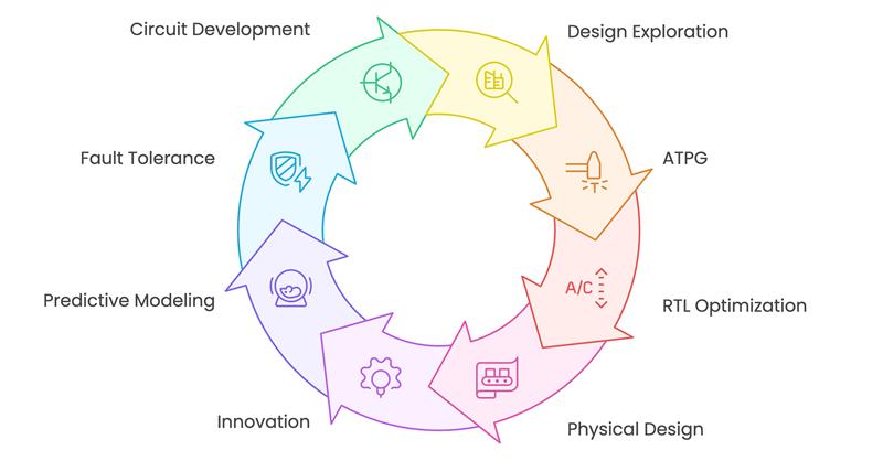
Let’s dive deeper into how these smart techniques are reshaping each functional area:
Design Exploration
AI techniques, such as genetic algorithms and evolutionary learning, can be used to optimize various aspects of VLSI design. Furthermore, AI aids in determining critical paths and how to accomplish less power consumption in VLSI. techniques, like frequency scaling and dynamic voltage, can be improved with AI.
For example, Google’s RL-based floorplanning approach showed up to 20% reduction in wirelength, demonstrating how AI can optimize design exploration more efficiently than manual methods.
Automatic Test Pattern Generation (ATPG)
It is an EDA methodology used to identify an input or test sequence. ATPG validates the correct circuit behaviour and the faulty circuit behaviour caused by defects. The patterns obtained are used to test semiconductors. However, the effectiveness of ATPG is a concern. AI in VLSI verification can automate the generation of advanced test patterns, improving coverage, speed, and reliability in semiconductor testing. AI-based pattern analysis can also highlight high-risk fault regions, allowing ATPG tools to target them more intelligently.
RTL Design Optimization (RTL)
AI can automate operations, such as datapath optimization and resource allocation. Hence, helps optimize RTL. ML algorithms can comprehend the design specification, performance goals, etc. Certain ML models can predict timing violations directly from RTL with around 85–90% accuracy, helping designers address issues before synthesis begins.
Physical Design Enhancement
AI in VLSI physical design plays a transformative role in improving physical design operations such as routing, placement, and floor planning. Moreover, ML algorithms can optimize chip layout, enhance timing closure, and minimize wavelength. There are other design challenges, like signal integrity analysis and clock tree synthesis, where AI can assist. For instance, the AI algorithm considers the factors skew and power consumption for clock tree structures.
Fast Design Exploration and Innovation
AI-driven behavioral synthesis tools have introduced high-level abstractions that allow designers to work at a more abstract level, focusing on functionality rather than low-level details. This shift in perspective enables faster design exploration and innovation. Machine learning models can learn from existing designs and propose high-level structures that match desired functionalities. This streamlines the design process and facilitates the exploration of diverse design alternatives, leading to more creative and efficient solutions.
Predictive Modeling and Fault Tolerance:
AI plays a crucial role in predictive modelling for VLSI designs. Predictive models, often based on neural networks, can estimate the performance of a design before it is physically implemented. This capability helps designers identify potential issues early in the design phase, reducing the need for costly redesigns. Moreover, AI contributes to fault tolerance in VLSI designs. By analyzing historical data on failures and learning from them, AI algorithms can suggest design modifications or redundancies to enhance integrated circuits’ robustness against various faults. These predictive insights help avoid late-stage design surprises, improving overall design reliability.
Analog and Digital Circuit Development
AI is helpful in analog and digital VLSI circuit design. In digital circuit design, AI can aid in logic synthesis and analog circuit design, AI can help in sizing transistors. For example, AI-based analog sizing tools have shown up to 20–30% reduction in simulation iterations, making the design process noticeably faster. In digital circuits, ML-driven logic optimization has demonstrated 5–10% improvement in timing slack by learning patterns from previous timing closure results.
Memory Testing in Digital VLSI Designs and its implications.

AI/ML Algorithms and Applications in VLSI Design and Technology
The integration of AI/ML algorithms and applications in VLSI design and technology has led to a paradigm shift in how chips are conceived, verified, and implemented. Here’s how these technologies are shaping the landscape:
- Pattern Recognition in Design Verification: Machine learning models can detect anomalies, bugs, or redundant logic patterns faster than manual inspection.
- Predictive Analysis: AI models anticipate power and performance bottlenecks early in the design phase, allowing proactive optimization.
- Intelligent Placement and Routing: ML algorithms learn from thousands of prior layouts to automatically suggest efficient chip placement strategies.
- Data-Driven Optimization: With AI-driven analytics, designers can make data-backed decisions that improve yield and reduce design iterations.
These applications collectively enhance design productivity and reliability, reducing the time-to-market for complex semiconductor systems.
Why are Efficient RTL Design Strategies for VLSI Integration important?
What’s Next for AI in VLSI? Emerging Trends
AI’s role in semiconductor design is rapidly expanding, and several emerging trends are shaping the next generation of chip development:
- Reinforcement Learning for Layout Optimization: RL models learn optimal placement strategies through continuous iteration, improving PPA (Power, Performance, Area).
- AI-Assisted Sign-Off: Predictive models capable of estimating EM, IR drop, and thermal effects early in the design cycle.
- Generative AI for Design Automation: GenAI models can generate RTL templates, propose microarchitecture variations, and accelerate early-stage design exploration.
- Autonomous Verification Environments: AI-enabled environments that continuously generate, analyze, and optimize test scenarios without manual intervention.
- Cross-Domain Co-Optimization: AI linking architecture decisions, power intent, and RTL implementation to ensure system-level efficiency.
Tessolve: Your Partner for Innovative Chip Design
The integration of AI into VLSI design has ushered in a new era of innovation and efficiency. From optimizing power consumption to automating complex design processes, AI has become an indispensable tool for semiconductor designers. The synergy between human creativity and AI-driven optimization is propelling VLSI circuit design to new heights, enabling the development of faster, more efficient, and reliable integrated circuits.
We at Tessolve provide VLSI chip design services encompassing RTL design, DV, emulation, FPGA, physical design, DFT, etc. We prioritize quality, reliability, and cost efficiency. Our VLSI team of 900 engineers delivers specs to GDSII solutions to our customers. Apart from this, we also provide end-to-end ASIC development services with our post-silicon engineering solutions. Furthermore, our IC capability includes:
- Analog and mixed-signal
- Design for Test (DFT)
- RTL and Physical design
- Design Verification (DV)
- FPGA Emulation and Validation
As AI continues to evolve, its impact on VLSI design is expected to grow, promising a future where the boundaries of what is possible in semiconductor design are continually pushed. With platforms like Tessolve, you can reap the maximum benefits out of VLSI chip design.
FAQs
How is AI transforming VLSI design?
AI automates design, optimization, and verification, improving efficiency, accuracy, and overall semiconductor performance.
What are the applications of AI/ML in VLSI design and technology?
AI/ML algorithms optimize chip layout, enhance verification, predict failures, and accelerate complex design processes.
Will AI replace VLSI engineers?
No, AI assists engineers by automating repetitive tasks while enabling smarter, faster design decisions.
How does AI improve physical design in VLSI?
AI enhances placement, routing, and timing closure, reducing design time and improving chip performance.