In recent years, the field of power electronics has undergone a significant transformation. Traditional silicon-based devices are increasingly being pushed to their operational limits regarding voltage, frequency, thermal stress, and efficiency. In this context, wide-bandgap semiconductors, particularly Silicon Carbide (SiC) and Gallium Nitride (GaN), have emerged as critical components for addressing these limitations. They play a pivotal role in facilitating the development of the next generation of high-performance and energy-efficient systems.
In addition to material advances, pre-silicon engineering activities, such as architecture definition, simulation, and functional verification, are crucial for unlocking the true potential of SiC and GaN technologies before fabrication begins. These steps ensure robust performance under harsh operating conditions and allow for early detection and correction of design flaws, significantly minimizing costly silicon re-spins.
What are Wide-Bandgap Semiconductors?
A “bandgap” in a semiconductor is the energy required to excite electrons from the valence band to the conduction band. A wider bandgap means the material can handle higher voltage, higher temperature, faster switching, and often exhibits lower leakage currents. SiC has a bandgap of around 3.3 eV, GaN about 3.4 eV, compared to silicon’s ~1.1 eV. These materials allow devices to function under harsher conditions than silicon ever could.
Before SiC and GaN devices reach production, modeling and simulation at the pre-silicon stage allow engineers to accurately predict switching behavior, thermal profiles, and system efficiency across varied application scenarios. This front-loaded approach ensures reliable designs and optimal component selection for demanding power electronics landscapes.
Key Advantages of SiC and GaN
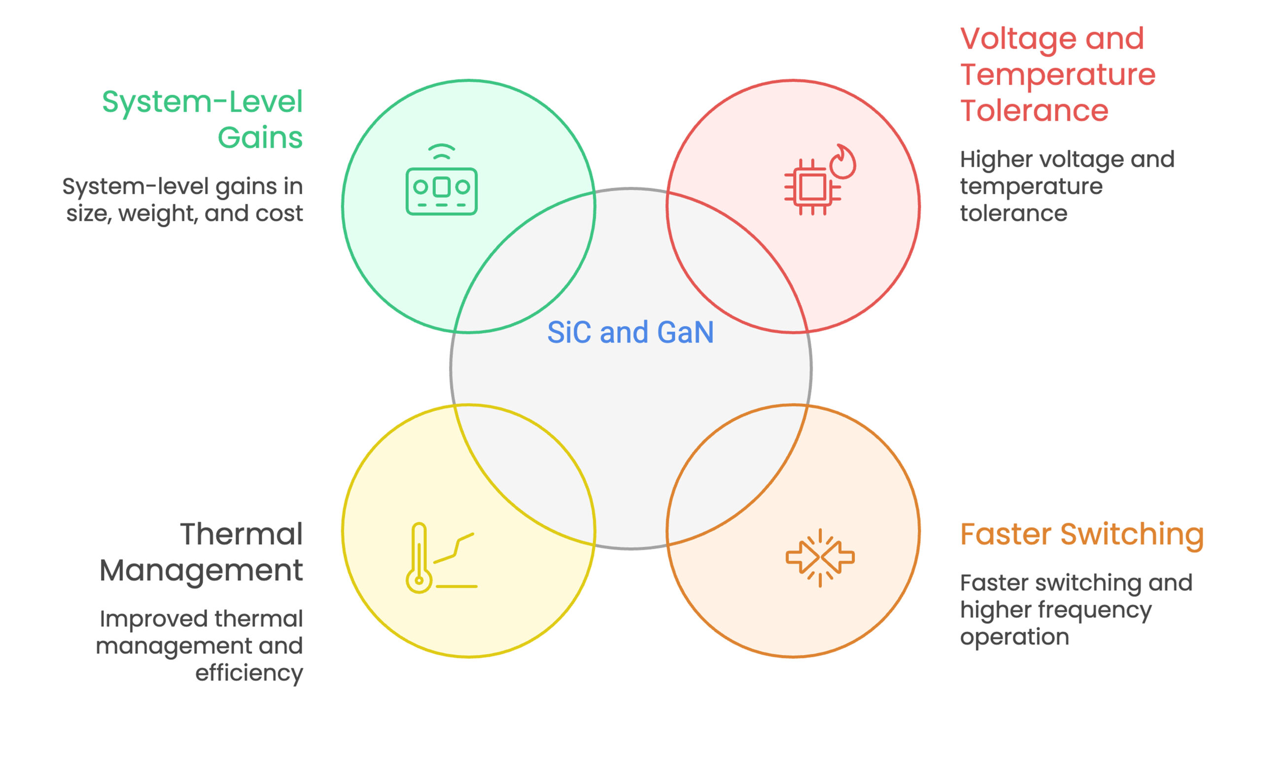
SiC and GaN each bring distinct benefits that give them a clear edge over traditional silicon-based devices. Below are the key advantages that make these wide-bandgap semiconductors transformative in power electronics:
1. Higher Voltage and Temperature Tolerance
SiC devices tolerate voltages of 600 V, 1200 V, or even up to 1700 V in many power conversion systems, with lower leakage and better robustness at elevated temperatures. GaN, while more commonly used in slightly lower voltage regions, excels in handling temperature due to its intrinsic physical properties.
2. Faster Switching, Higher Frequency Operation
GaN devices enable switching in the MHz range, greatly shrinking the size of passive components (inductors, capacitors) and overall system size. SiC also improves switching speed and allows for designs with fewer losses when operating at higher frequencies.
3. Improved Thermal Management and Efficiency
One of the obstacles in high-power systems is the generation and removal of heat. SiC has high thermal conductivity; GaN devices, because they switch more cleanly and efficiently, produce less heat under comparable load. Less wasted energy as heat translates to smaller heatsinks, better reliability, and compact systems.
4. System-Level Gains in Size, Weight, and Cost
Even though SiC and GaN semiconductors tend to have higher upfront device cost compared to silicon, at the system level, the savings in reduced cooling, smaller magnetics, lighter weight, and greater energy conversion efficiency often outweigh those costs. This is especially true in EVs, renewable energy inverters, data centers, and industrial drives.
Comparative Performance of Si, SiC, and GaN in Power Electronics
| Parameter | Silicon (Si) | Silicon Carbide (SiC) | Gallium Nitride (GaN) |
| Bandgap (eV) | ~1.1 | ~3.3 | ~3.4 |
| Max Operating Temperature | 150°C | 250–300°C | 200–250°C |
| Breakdown Voltage | 600–1200V (typical) | 600–1700V (high voltage applications) | 200–650V (typical) |
| Switching Frequency | Up to ~100 kHz | 100 kHz–1 MHz | 1–10 MHz (high frequency) |
| Thermal Conductivity | 150 W/m·K | 300 W/m·K | 130–200 W/m·K |
| On-Resistance (Rds(on)) | Moderate | Low | Very Low (for high-frequency) |
| Efficiency at High Power | Moderate | High | Very High |
| Leakage Current | Moderate | Low | Very Low |
| System Size & Weight | Larger | Reduced (smaller heatsinks & magnetics) | Significantly reduced (high-frequency operation) |
| Cost | Low | High | Moderate (falling with adoption) |
| Typical Applications | Consumer electronics, standard power supplies | EV inverters, industrial drives, and renewable energy | Fast chargers, telecom RF, data center power supplies |
Where SiC and GaN are Making the Biggest Impact
The real power of wide-bandgap semiconductors is visible in the industries where they are being deployed today. Here are some of the sectors that benefit most from SiC and GaN adoption:
- Electric Vehicles (EVs): EV powertrains are adopting SiC MOSFETs and SiC-based inverters for higher voltage architectures (e.g., 800V systems), which deliver better range, faster charging, and lighter weight.
- Renewable Energy & Grid: Solar inverters, wind turbine converters, and grid-scale power converters benefit from SiC because losses at high voltage and high current are major sources of inefficiency.
- Data Centers & Telecom: GaN excels in power supplies and delivery in data centers. Its high switching frequency allows more compact supplies, less heat, and better power density. For 5G base stations, fast chargers, and RF amplifiers, GaN is increasingly the go-to.
- Industrial & Aerospace: Harsh environments, high temperature, and weight constraints make both SiC and GaN favorable in industrial machine drives, aviation systems, and defense electronics.
Challenges & Design Considerations
While SiC and GaN offer tremendous benefits, adopting them at scale requires addressing several practical challenges. Below are some of the most important considerations for engineers and manufacturers:
- Cost & Manufacturing Yield: WBG materials are more expensive to produce; defects in the crystal lattice (especially for SiC) or in GaN growth can reduce yield.
- Packaging & Thermal Interfaces: To fully leverage the advantages, packaging must also be adapted for better thermal paths, reduce parasitics, and use robust materials.
- Gate Drive & Control Circuits: High switching frequency devices require an advanced gate driver design to manage EMI and ringing.
- Reliability & Standards: Long-term robustness of GaN in some applications is still under study; SiC is more mature for high-voltage systems.
Developing automated test strategies and reliability schemes during pre-silicon activities ensures a smooth transition from design to mass production and long-term operation of SiC/GaN-powered systems.
Role of Design, Engineering, and Collaboration
The advantages of SiC and GaN create opportunities but also demand new design practices. This isn’t about simply swapping silicon for WBG devices; it requires rethinking PCB layout, drivers, thermal strategies, and compliance. That’s where collaboration with a top semiconductor company, a strong semiconductor design company, and providers of semiconductor engineering services becomes vital. Together, they make wide-bandgap adoption practical and scalable for mass markets.
By focusing on pre-silicon modeling, simulation, FPGA prototyping, and early test planning, semiconductor design teams, supported by Tessolve, achieve reliable, high-performance, and competitive products in SiC and GaN markets.
Future Trends in SiC and GaN Adoption
The wide-bandgap revolution is still unfolding, and several key trends are shaping its trajectory:
- EV Expansion: SiC inverters and GaN onboard chargers will dominate as global EV adoption accelerates.
- Fast Charging Infrastructure: High-efficiency chargers built on SiC/GaN enable ultra-fast charging at scale.
- 5G & Beyond: GaN devices are crucial in high-frequency RF front-ends for telecom and satellite.
- Energy Transition: Renewable integration into smart grids demands SiC for efficiency and stability.
- Miniaturization: Consumer electronics increasingly rely on GaN for compact, fast-charging adapters.
- Cost Reduction: As volumes rise, manufacturing improvements will lower costs and boost accessibility.
These trends highlight why partnering with a semiconductor design company and experts in semiconductor engineering services is essential for staying competitive.
The Future of Semiconductor Design: How Emerging Technologies Are Shaping the Industry
Tessolve: Your Partner for Wide-Bandgap Success
At Tessolve, we provide end-to-end semiconductor solutions that empower companies to embrace the SiC and GaN revolution with confidence. Our expertise spans IC design, physical verification, FPGA prototyping, test engineering, and package & PCB design. With advanced reliability labs, qualification services, and system-level validation, we ensure that wide-bandgap devices meet performance, safety, and long-term reliability standards.
From pre-silicon design and simulation to post-silicon validation, Tessolve’s comprehensive engineering services enable clients to realize innovative SiC and GaN products faster and with minimized risk for automotive, renewable energy, telecom, and data center applications.
As a top semiconductor company offering world-class semiconductor design expertise and comprehensive semiconductor engineering services, Tessolve helps customers accelerate innovation, reduce time-to-market, and minimize risks in next-gen power electronics. Whether it’s automotive, renewable energy, telecom, or data center systems, we bring the experience and engineering excellence to transform your SiC and GaN designs into successful, field-ready products.